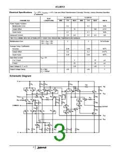
ICL8013
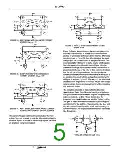
output of the modulator is again forced to equal the current
produced by the Z input.
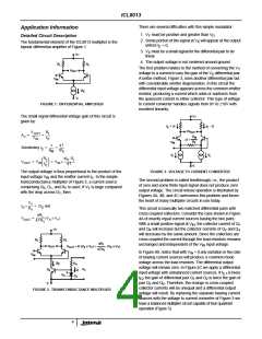
Z
IN
1
10
R =
I
Z
10Z
X
IN
V
=
2
OUT
I
= X × Y = (–V
)
= 10Z
IN
X
Y
O
IN
IN
OUT
IN
IN
IN
MODULATOR
OP AMP
I
O
V
= – 10Z
IN
OUT
The output is a negative voltage which maintains overall
negative feedback. A diode in series with the op amp output
prevents the latchup that would otherwise occur for negative
input voltages.
FIGURE 8A. DIVISION BLOCK DIAGRAM
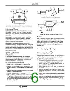
SQUARE ROOT TRIMMING PROCEDURE
X
7
Y
Z
OS OS OS
1. Connect the ICL8013 in the Divider configuration.
10
9
2. Adjust Z , Y , X , and Gain using Steps 1 through 6
OS OS OS
(0 TO -10V)
6
10Z
IN
X
Z
OUTPUT =
4
IN
IN
of Divider Trimming Procedure.
X
IN
ICL8013
3
1
3. Convert to the Square Root configuration by connecting
X
to the output and inserting a diode between Pin 4 and
IN
the output node.
Y
IN
5K
GAIN
4. With Z = 0V adjust Z
IN
for zero output voltage.
OS
7.5K
Z
1
10
R =
FIGURE 8B. DIVISION CIRCUIT CONNECTION
I
Z
X
IN
V
= -√10Z
OUT
IN
MODULATOR
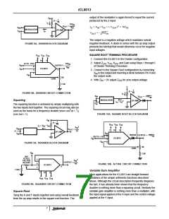
Squaring
OP AMP
2
I
= V
O
O
Y
IN
The squaring function is achieved by simply multiplying with
the two inputs tied together. The squaring circuit may also be
used as the basis for a frequency doubler since cos ωt = /
2
1
2
FIGURE 10A. SQUARE ROOT BLOCK DIAGRAM
(cos 2ωt + 1).
Z
IN
1
10
R =
X
7
Y
Z
OS OS OS
I
= X • Y
IN IN
O
2
X
IN
X
Y
IN
IN
V
=
OUT
10
9
10
X
OP AMP
X
IN
6
1N4148
4
OUTPUT = -√10Z
IN
(0V TO + 10V)
ICL8013
Z
IN
3
1
Y
IN
FIGURE 9A. SQUARER BLOCK DIAGRAM
5K
GAIN
X
IN
7.5K
5kΩ
SCALE
FACTOR
ADJUST
3
6
1
2
X
IN
OUTPUT =
10
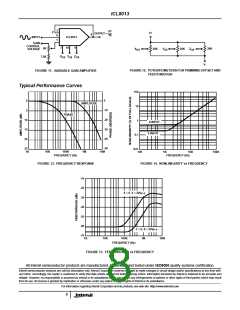
FIGURE 10B. ACTUAL CIRCUIT CONNECTION
ICL8013
4
7.5kΩ
Variable Gain Amplifier
7
10
9
Most applications for the ICL8013 are straight forward
variations of the simple arithmetic functions described
X
Y
Z
OS OS OS
above. Although the circuit description frequently disguises
the fact, it has already been shown that the frequency
doubIer is nothing more than a squaring circuit. Similarly the
variable gain amplifier is nothing more than a multiplier, with
the input signal applied at the X input and the control voltage
applied at the Y input.
FIGURE 9B. SQUARER CIRCUIT CONNECTION
Square Root
Tying the X and Y inputs together and using overall feedback
from the op amp results in the square root function. The
7

 INTERSIL [ Intersil ]