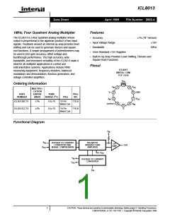
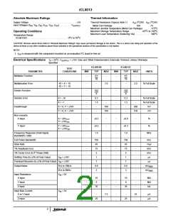
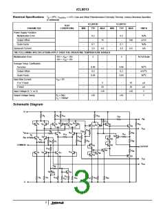
ICL8013
There are several difficulties with this simple modulator:
1. V must be positive and greater than V .
Application Information
Y
D
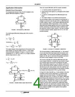
Detailed Circuit Description
2. Some portion of the signal at V will appear at the output
X
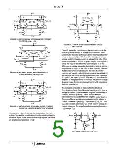
The fundamental element of the ICL8013 multiplier is the
bipolar differential amplifier of Figure 1.
unless I = 0.
E
3. V must be a small signal for the differential pair to be
X
V+
linear.
4. The output voltage is not centered around ground.
The first problem relates to the method of converting the V
R
R
L
L
Y
V
OUT
voltage to a current to vary the gain of the V differential pair.
X
A better method, Figure 3, uses another differential pair but
with considerable emitter degeneration. In this circuit the
differential input voltage appears across the common emitter
resistor, producing a current which adds or subtracts from
the quiescent current in either collector. This type of voltage
to current converter handles signals from 0V to ±10V with
excellent linearity.
V
IN
2I
E
V-
FIGURE 1. DIFFERENTIAL AMPLIFIER
V+
The small signal differential voltage gain of this circuit is
given by:
I
+ ∆I
I - ∆I
E
E
∆V
OUT
V
R
L
r
E
OUT
A
= --------------- = ------
V
V
IN
V
IN
∆I =
R
V
E
IN
1
kT
qI
E
Substituting r = ------- = --------
E
g
M
I
I
E
E
R
qI
R
E L
kT
L
------
------------------
×
IN
V
= V
= V
OUT
IN
r
E
V-
The output voltage is thus proportional to the product of the
FIGURE 3. VOLTAGE TO CURRENT CONVERTER
input voltage V and the emitter current I . In the simple
transconductance multiplier of Figure 2, a current source
lN
E
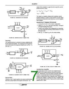
The second problem is called feedthrough; i.e., the product
of zero and some finite Input signal does not produce zero
output voltage. The circuit whose operation is illustrated by
Figures 4A, 4B, and 4C overcomes this problem and forms
the heart of many multiplier circuits in use today.
comprising Q , D , and R is used. If V is large compared
3
1
Y
Y
with the drop across D , then
1
V
Y
R
Y
-------
I
≈
= 2I and
D
E
This circuit is basically two matched differential pairs with
cross coupled collectors. Consider the case shown in Figure
4A of exactly equal current sources basing the two pairs.
qR
L
kTR
Y
---------------
(V × V )
X Y
V
=
OUT
With a small positive signal at V , the collector current of Q
lN
1
and Q will increase but the collector currents of Q and Q
V+
4
2
3
will decrease by the same amount. Since the collectors are
cross coupled the current through the load resistors remains
unchanged and independent of the V input voltage.
lN
R
R
L
L
qR
L
V
V
= K (V x V ) =
(V x V )
X Y
OUT
OUT
X
Y
kTR
Y
In Figure 4B, notice that with V = 0 any variation in the ratio
IN
V
IN
of biasing current sources will produce a common mode
voltage across the load resistors. The differential output
voltage will remain zero. In Figure 4C we apply a differential
2I
R
E
Y
V
Q
I
Y
3
D
+
-
input voltage with unbalanced current sources. If I is twice
E1
V
D
D
1
I
the gain of differential pair Q and Q is twice the gain of
1 2
E2
pair Q and Q . Therefore, the change in cross coupled
V-
3
4
collector currents will be unequal and a differential output
voltage will result. By replacing the separate biasing current
sources with the voltage to current converter of Figure 3 we
have a balanced multiplier circuit capable of four quadrant
operation (Figure 5).
FIGURE 2. TRANSCONDUCTANCE MULTIPLIER
4

 INTERSIL [ Intersil ]