ICL8013
Absolute Maximum Ratings
Thermal Information
o
o
Supply Voltage. . . . . . . . . . . . . . . . . . . . . . . . . . . . . . . . . . . . . . ±18
Thermal Resistance (Typical, Note 1)
Metal Can Package . . . . . . . . . . . . . . .
θ
( C/W)
θ
( C/W)
JA
JC
Input Voltages (X , Y , Z , X , Y , Z ) . . . . . . . . . V
IN IN IN OS OS OS
SUPPLY
160
75
o
Maximum Junction Temperature (Metal Can Package) . . . . . . .175 C
Maximum Storage Temperature Range. . . . . . . . . . -65 C to 150 C
Maximum Lead Temperature (Soldering 10s) . . . . . . . . . . . . 300 C
o
o
Operating Conditions
o
Temperature Range
o
o
ICL8013XC. . . . . . . . . . . . . . . . . . . . . . . . . . . . . . . . 0 C to 70 C
CAUTION: Stresses above those listed in “Absolute Maximum Ratings” may cause permanent damage to the device. This is a stress only rating and operation of the
device at these or any other conditions above those indicated in the operational sections of this specification is not implied.
NOTE:
1. θ is measured with the component mounted on an evaluation PC board in free air.
JA
o
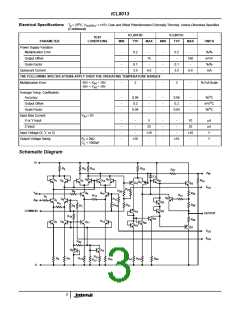
Electrical Specifications T = 25 C, V
= ±15V, Gain and Offset Potentiometers Externally Trimmed, Unless Otherwise
SUPPLY
A
Specified
ICL8013B
TYP
ICL8013C
TYP
TEST
CONDITIONS
PARAMETER
MIN
MAX
MIN
MAX
UNITS
Multiplier Function
-
XY
10
-
-
XY
10
-
Multiplication Error
Divider Function
-10 < X < 10
-10 < Y < 10
-
-
-
1.0
-
-
-
-
2.0
-
% Full Scale
10Z
X
10Z
X
Division Error
Feedthrough
X = -10
-
-
-
-
0.3
1.5
-
-
-
-
-
-
0.3
1.5
-
-
% Full Scale
% Full Scale
mV
X = -1
-
-
X = 0, Y = ±10V
Y = 0, X = ±10V
100
100
200
150
-
-
mV
Non-Linearity
X Input
X = 20V
Y= ±10V
-
-
-
±0.5
±0.2
1.0
-
-
-
-
-
-
±0.8
±0.3
1.0
-
-
-
%
%
P-P
DC
Y Input
Y = 20V
P-P
X = ±10V
DC
Frequency Response Small Signal
Bandwidth (-3dB)
MHz
Full Power Bandwidth
Slew Rate
-
-
-
-
-
-
-
-
750
45
75
5
-
-
-
-
-
-
-
-
-
-
-
-
-
-
-
-
750
45
75
5
-
-
-
-
-
-
-
-
kHz
V/µs
kHz
kHz
µs
1% Amplitude Error
o
1% Vector Error (0.5 Phase Shift)
Settling Time (to ±2% of Final Value)
V
= ±10V
1
1
lN
Overload Recovery (to ±2% of Final Value) V = ±10V
lN
1
1
µs
Output Noise
5Hz to 10kHz
5Hz to 5MHz
0.6
3
0.6
3
mV
mV
RMS
RMS
Input Resistance
X lnput
V
= 0V
lN
-
-
-
10
6
-
-
-
-
-
-
10
6
-
-
-
MΩ
Y lnput
Z lnput
MΩ
kΩ
36
36
Input Bias Current
X or Y Input
V
= 0V
lN
-
-
-
7.5
-
-
-
-
10
-
µA
µA
Z Input
25
25
2

 INTERSIL [ Intersil ]