ICL8013
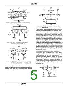
Z
IN
1
10
V+
R =
X
Y
IN IN
I
= X • Y
IN IN
V
=
O
OUT
10
X
IN
V
MODULATOR
OUT
OP AMP
Y
IN
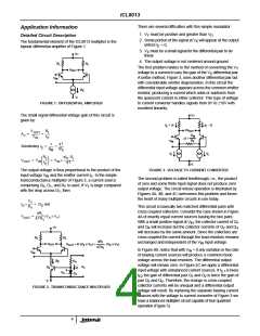
FIGURE 7A. MULTIPLIER BLOCK DIAGRAM
V-
V-
V
IN
X
Y
IN IN
OUTPUT =
3
6
1
Z
10
IN
4
ICL8013
X
IN
Y
IN
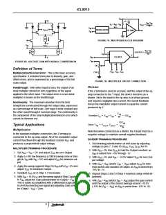
FIGURE 6B. VOLTAGE GAIN WITH SIGNAL COMPRESSION
7
10
9
5K
Definition of Terms
X
Y
Z
OS OS OS
7.5K
Multiplication/Division Error: This is the basic accuracy
specification. It includes terms due to linearity, gain, and
offset errors, and is expressed as a percentage of the full
scale output.
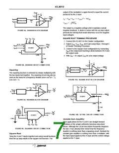
FIGURE 7B. MULTIPLIER CIRCUIT CONNECTION
Division
Feedthrough: With either input at zero, the output of an
ideal multiplier should be zero regardless of the signal
applied to the other input. The output seen in a non-ideal
multiplier is known as the feedthrough.
If the Z terminal is used as an input, and the output of the op
amp connected to the Y input, the device functions as a
divider. Since the input to the op amp is at virtual ground,
and requires negligible bias current, the overall feedback
forces the modulator output current to equal the current
produced by Z.
Nonlinearity: The maximum deviation from the best
straight line constructed through the output data, expressed
as a percentage of full scale. One input is held constant and
the other swept through it nominal range. The nonlinearity is
the component of the total multiplication/division error which
cannot be trimmed out.
Z
IN
Therefore I = X • Y
= --------- = 10Z
O
IN
IN
IN
R
10Z
IN
Since Y
= V
, V
OUT OUT
= ----------------
Typical Applications
IN
X
IN
Multiplication
Note that when connected as a divider, the X input must be a
negative voltage to maintain overall negative feedback.
In the standard multiplier connection, the Z terminal is
connected to the op amp output. All of the modulator output
current thus flows through the feedback resistor R and
DIVIDER TRIMMING PROCEDURE
27
1. Set trimming potentiometers at mid-scale by adjusting
produces a proportional output voltage.
voltage on pins 7, 9 and 10 (X , Y , Z ) for 0V.
OS OS OS
MULTIPLIER TRIMMING PROCEDURE
2. With Z = 0V, trim Z
IN
to hold the Output constant, as
OS
is varied from -10V through -1V.
1. Set X = Y = 0V and adjust Z
IN IN OS
for zero Output.
X
IN
2. Apply a ±10V low frequency (≤100Hz) sweep (sine or trian-
gle) to Y with X = 0V, and adjust X for minimum out-
3. With Z = 0V and X = -10.0V adjust Y for zero Out-
IN
IN
OS
IN IN OS
put voltage.
put.
4. With Z = X (and/or Z = -X ) adjust X
IN IN IN IN
for mini-
OS
3. Apply the sweep signal of Step 2 to X with Y = 0V and
IN IN
mum worst case variation of Output, as X is varied from
IN
adjust Y
for minimum Output.
OS
-10V to -1V.
4. Readjust Z
as in Step 1, if necessary.
OS
5. Repeat Steps 2 and 3 if Step 4 required a large initial ad-
justment.
5. With X = 10.0V and the sweep signal of Step 2 applied
IN DC
to Y , adjust the Gain potentiometer for Output = Y .
This is easily accomplished with a differential scope plug-
in (A+B) by inverting one signal and adjusting Gain control
IN IN
6. With Z = X (and/or Z = -X ) adjust the gain control
IN IN IN IN
until the output is the closest average around +10.0V
(-10V for Z = -X ) as X is varied from -10V to -3V.
IN IN IN
for (Output - Y ) = Zero.
IN
6

 INTERSIL [ Intersil ]