ICL8013
V+
V+
R
L
R
R
R
L
I
I
L
E
E
∆V = K • (V • V )
X
Y
∆V
OUT
= 0
1
1
1
1
/
I
+ ∆
/ I + ∆
2 E
2
E
/
I
- ∆
/ I - ∆
2 E
2 E
+
+
Q
Q
Q
Q
4
1
2
3
Q
Q
Q
Q
4
1
2
3
V
IN
-
V
IN
-
R
E
I
I
E
E
V
IN
V-
I
I
E
E
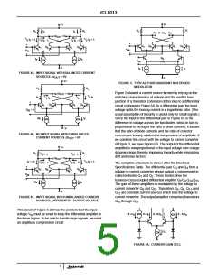
FIGURE 4A. INPUT SIGNAL WITH BALANCED CURRENT
SOURCES ∆V
= 0V
OUT
V-
V+
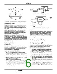
FIGURE 5. TYPICAL FOUR QUADRANT MULTIPLIER-
MODULATOR
R
R
L
L
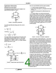
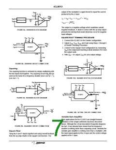
Figure 2 showed a current source formed by relying on the
matching characteristics of a diode and the emitter base
junction of a transistor. Extension of this idea to a differential
circuit is shown in Figure 6A. In a differential pair, the input
voltage splits the biasing current in a logarithmic ratio. (The
usual assumption of linearity is useful only for small signals.)
Since the input to the differential pair in Figure 6A is the
difference in voltage across the two diodes, which in turn is
proportional to the log of the ratio of drive currents, it follows
that the ratio of diode currents and the ratio of collector
currents are linearly related and independent of amplitude. If
we combine this circuit with the voltage to current converter
of Figure 3, we have Figure 6B. The output of the differential
amplifier is now proportional to the input voltage over a large
dynamic range, thereby improving linearity while minimizing
drift and noise factors.
∆V
= 0
OUT
1
1
I
/ I
2 E
E
/
I
I
E
2 E
+
Q
Q
Q
Q
4
1
2
3
V
= 0
IN
-
2I
I
E
E
V-
FIGURE 4B. NO INPUT SIGNAL WITH UNBALANCED
CURRENT SOURCES ∆V
= 0V
OUT
V+
R
R
L
3
3
/ I - ∆
L
/ I + ∆
2
2
∆V
OUT
= 0
1
1
1
I
+ 2∆
/ I + ∆
2 E
E
/
I
- ∆
/ I - 2∆
2 E
2 E
The complete schematic is shown after the Electrical
+
Specifications Table. The differential pair Q and Q form a
3
4
Q
Q
Q
Q
4
1
2
3
voltage to current converter whose output is compressed in
collector diodes Q and Q . These diodes drive the
V
IN
1
2
-
balanced cross-coupled differential amplifier Q /Q Q /Q
.
7
8
14 15
2I
I
E
E
The gain of these amplifiers is modulated by the voltage to
current converter Q and Q . Transistors Q , Q , Q , and
9
10 11
5
6
V-
Q
are constant current sources which bias the voltage to
12
current converter. The output amplifier comprises transistors
FIGURE 4C. INPUT SIGNAL WITH UNBALANCED CURRENT
SOURCES, DIFFERENTIAL OUTPUT VOLTAGE
Q
through Q .
27
16
This circuit of Figure 5 still has the problem that the input
X x I
D
X x I
(I - X) I
(I - X) I
D
voltage V must be small to keep the differential amplifier in
E
E
IN
the linear region. To be able to handle large signals, we need
an amplitude compression circuit.
2 I
E
FIGURE 6A. CURRENT GAIN CELL
5

 INTERSIL [ Intersil ]