HA-2420, HA-2425
INPUT
Application Information
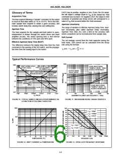
HOLD STEP VOLTAGE (mV)
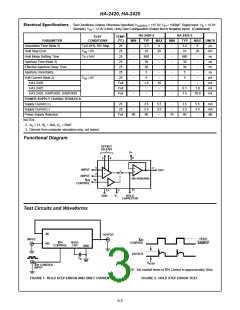
+10
OUTPUT
+IN
-IN
OUT
S/H
CONTROL
5
R
F
-10
-5
+5
+10
S/H CONTROL
INPUT
R
I
0
R
F
DC INPUT VOLTAGE (V)
NOTE: GAIN ~ 1 + -------
0.002R
I
-5
R
I
C
= 0.1µF
H
-10
C
C
= 10,000pF
= 1000pF
H
H
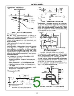
FIGURE 7. NON-INVERTING CONFIGURATION
-15
-20
-25
-30
-35
Figure 8 shows a typical unity gain circuit, with Offset Zero-
ing. All of the other normal op amp feedback configurations
may be used with the HA-2420/2425. The input amplifier
may be used as a gated amplifier by utilizing Pin 11 as the
output. This amplifier has excellent drive capabilities along
with exceptionally low switch leakage.
C
= 100pF
H
CONTROL
FIGURE 5. HOLD STEP vs INPUT VOLTAGE
V+
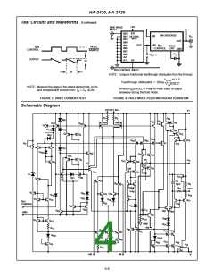
Offset Adjustment
C
H
The offset voltage of the HA-2420 and HA-2425 may be
adjusted using a 100kΩ trim pot, as shown in Figure 8. The
recommended adjustment procedure is:
Apply 0V to the sample-and-hold input, and a square wave
to the S/H control.
-
+
-
+
Adjust the trim pot for 0V output in the hold mode.
Gain Adjustment
The linear variation in pedestal voltage with sample-and- hold
OUT
input voltage causes a -0.06% gain error (C = 1000pF). In
IN
100kΩ
V-
H
some applications (D/A deglitcher, A/D converter) the gain
error can be adjusted elsewhere in the system, while in other
applications it must be adjusted at the sample-and-hold. The
two circuits shown below demonstrate how to adjust gain error
at the sample-and-hold.
OFFSET TRIM (±25mV RANGE)
FIGURE 8. BASIC SAMPLE-AND-HOLD (TOP VIEW)
The method used to reduce leakage paths on the PC board
and the device package is shown in Figure 9. This guard ring
is recommended to minimize the drift during hold mode.
The recommended procedure for adjusting gain error is:
1. Perform offset adjustment.
The hold capacitor should have extremely high insulation
resistance and low dielectric absorption. Polystyrene (below
2. Apply the nominal input voltage that should produce a
+10V output.
o
85 C), Teflon, or Parlene types are recommended.
3. Adjust the trim pot for +10V output in the hold mode.
For more applications, consult Intersil Application Note
AN517, or the factory applications group.
4. Apply the nominal input voltage that should produce a
-10V output.
CONTROL
5. Measure the output hold voltage (V
-10NOMINAL
). Adjust
GND
the trim pot for an output hold voltage of
-IN
+IN
(V–10NOMINAL) + (-10V)
HOLD
CAPACITOR
----------------------------------------------------------------------------
2
R
0.002R
OUT
F
F
INPUT
R
OUTPUT
I
V-
OUT
-IN
S/H
CONTROL
V+
+IN
–R
F
R
I
----------
NOTE: GAIN
S/H CONTROL INPUT
FIGURE 9. GUARD RING LAYOUT (BOTTOM VIEW)
FIGURE 6. INVERTING CONFIGURATION
5-5

 INTERSIL [ Intersil ]