HA-2420, HA-2425
Absolute Maximum Ratings
Thermal Information
o
o
Voltage Between V+ and V- Terminals . . . . . . . . . . . . . . . . . . . . 40V
Differential Input Voltage. . . . . . . . . . . . . . . . . . . . . . . . . . . . . . . 24V
Digital Input Voltage (Sample and Hold Pin) . . . . . . . . . . +8V, -15V
Output Current . . . . . . . . . . . . . . . . . . . . . . . Short Circuit Protected
Thermal Resistance (Typical, Note 1)
θ
( C/W)
θ
( C/W)
JA
JC
CERDIP Package . . . . . . . . . . . . . . . . . .
PDIP Package . . . . . . . . . . . . . . . . . . . . .
PLCC Package . . . . . . . . . . . . . . . . . . . .
SOIC Package. . . . . . . . . . . . . . . . . . . . .
90
100
75
35
N/A
N/A
120
N/A
o
Maximum Junction Temperature (Ceramic Packages) . . . . . . . 175 C
Maximum Junction Temperature (Plastic Package) . . . . . . . . 150 C
Maximum Storage Temperature Range . . . . . . . . . -65 C to 150 C
Maximum Lead Temperature (Soldering 10s). . . . . . . . . . . . . 300 C
Operating Conditions
o
Temperature Range
HA-2420-2. . . . . . . . . . . . . . . . . . . . . . . . . . . . . . -55 C to 125 C
HA-2425-5. . . . . . . . . . . . . . . . . . . . . . . . . . . . . . . . . 0 C to 75 C
o
o
o
o
o
o
o
(PLCC and SOIC - Lead Tips Only)
Supply Voltage Range (Typical) . . . . . . . . . . . . . . . . . ±12V to ±15V
CAUTION: Stresses above those listed in “Absolute Maximum Ratings” may cause permanent damage to the device. This is a stress only rating and operation
of the device at these or any other conditions above those indicated in the operational sections of this specification is not implied.
NOTE:
1. θ is measured with the component mounted on an evaluation PC board in free air.
JA
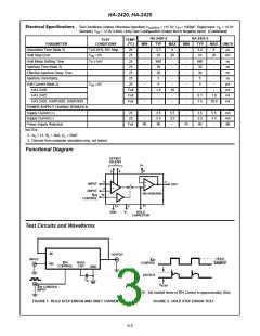
Electrical Specifications Test Conditions (Unless Otherwise Specified) V
= ±15.0V; C = 1000pF; Digital Input: V = +0.8V
(Sample), V = +2.0V (Hold), Unity Gain Configuration (Output tied to Negative Input)
SUPPLY
H
IL
IH
HA-2420-2
TYP
HA-2425-5
TYP
TEST
CONDITIONS
TEMP.
( C)
o
PARAMETER
INPUT CHARACTERISTICS
Input Voltage Range
MIN
MAX
MIN
MAX UNITS
Full
25
±10
-
2
-
4
±10
-
3
-
6
V
Offset Voltage
-
-
mV
mV
nA
nA
nA
nA
MΩ
V
Full
25
-
3
6
-
4
8
Bias Current
-
40
-
200
400
50
100
-
-
40
-
200
400
50
100
-
Full
25
-
-
Offset Current
-
-
10
-
-
-
10
-
Full
25
Input Resistance
5
10
-
5
10
-
Common Mode Range
Full
±10
-
±10
-
TRANSFER CHARACTERISTICS
Large Signal Voltage Gain
Common Mode Rejection
R = 2kΩ, V = 20V
Full
Full
Full
25
80
-
50
90
-
-
-
25
74
-
50
90
-
-
-
kV/V
dB
L
O
P-P
V
= ±10V
CM
Hold Mode Feedthrough Attenuation
(Note 2)
f
≤ 100kHz
-76
-76
dB
IN
Gain Bandwidth Product (Note 2)
OUTPUT CHARACTERISTICS
Output Voltage Swing
25
-
2.5
-
-
2.5
-
MHz
R = 2kΩ
Full
25
±10
-
-
-
-
-
±10
-
-
-
-
-
V
mA
kHz
Ω
L
Output Current
±15
-
±15
-
Full Power Bandwidth (Note 2)
Output Resistance
V
= 20V
P-P
25
-
-
100
0.15
-
-
100
0.15
O
DC
25
TRANSIENT RESPONSE
Rise Time (Note 2)
V
= 200mV
V = 200mV
O
25
25
25
-
-
75
25
5
100
40
-
-
-
75
25
5
100
40
-
ns
%
O
P-P
Overshoot (Note 2)
P-P
Slew Rate (Note 2)
V
= 10V
3.5
3.5
V/µs
O
P-P
DIGITAL INPUT CHARACTERISTICS
Digital Input Current
V
V
= 0V
= 5V
Full
Full
Full
Full
-
-
-
-
-
-
-0.8
20
0.8
-
-
-
-
-
-
-
-0.8
20
0.8
-
mA
µA
V
IN
IN
Digital Input Voltage
Low
-
-
High
2.0
2.0
V
SAMPLE AND HOLD CHARACTERISTICS
Acquisition Time (Note 2) To 0.1% 10V Step
25
-
2.3
4
-
2.3
4
µs
5-2

 INTERSIL [ Intersil ]