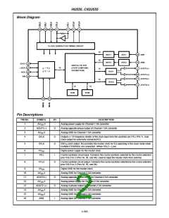
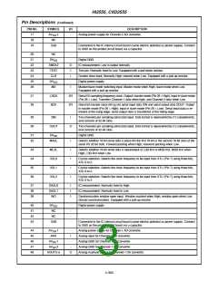
HI2555, CXD2555
o
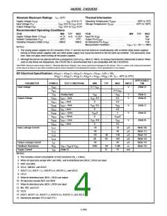
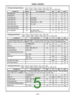
Absolute Maximum Ratings
T
= 25 C
Thermal Information
A
o
o
o
Supply Voltage (V ). . . . . . . . . . . . . . . . . . . . . . . .V -0.5V to 7V
Operating Temperature (T
) . . . . . . . . . . . . . . . . .-20 C to 75 C
DD SS
OPR
Storage Temperature (T ) . . . . . . . . . . . . . . . . . .-55 C to 150 C
STG
o
Input Voltage (V ). . . . . . . . . . . . . . . . . . . . V -0.5V to V
SS
+0.5V
+0.5V
1
DD
DD
Output Voltage (V ) . . . . . . . . . . . . . . . . . . V -0.5V to V
0
SS
Recommended Operating Conditions
ITEM
MIN
TYP
MAX
ITEM
MIN
TYP
MAX
9pF
11pF
11pF
Supply Voltage (Note 1) (V ). . . . . . . . . . . +4.75 +5.0 +5.25V
Input Pin (C ). . . . . . . . . . . . . . . . . . . . . . .
Output Pin (C
Bi-Directional Pin (C ) . . . . . . . . . . . . . . .
-
-
-
-
-
-
DD
Ambient Temperature (T ). . . . . . . . . . . . . . -20 C
IN
o
o
-
-
75 C
. . . . . . . . . . . . . . . . . . . .
OUT
A
Sampling Frequency (Note 2) (f ) . . . . . . . .30kHz
50kHz
S
I/O
Measurement Conditions . . . . . . . . . . . . . V
= V = 0V, f = 1MHz
DD
I
NOTES:
1. The analog power supplies for AD converters (Pins 17 and 44) must be turned on simultaneously with or before other power supplies.
turning on these power supplies after any other power supply may cause the device to fall into latch-up condition. This precaution, how-
ever, does not apply when turning off the power supplies.
2. Although the device can operate with low f frequencies such as f = 8kHz or 16kHz, its analog characteristics deteriorate to extent. When
S
S
used at only these low frequencies, the CXD2570Q is recommended that is pin-compatible with the CXD2555Q.
CAUTION: Stresses above those listed in “Absolute Maximum Ratings” may cause permanent damage to the device. This is a stress only rating and operation
of the device at these or any other conditions above those indicated in the operational sections of this specification is not implied.
DC Electrical Specifications (AV 1 = AV 2 = AV 3 = AV 4 = XV
= 5.0V ± 10%,
DD
DD
SS
DD
SS
DD
DD
o
o
AV 1 = AV
2 = AV
3 = AV 4 = XV = DV = 0V, T = -20 C to 75 C)
SS
SS
SS
SS
A
APPLICABLE
PIN
PARAMETER
Input Voltage
SYMBOL
TEST CONDITIONS
MIN
TYP
MAX
UNITS
V
0.7 V
-
-
V
(Note 4)
IHC
DD
V
-
-
0.3 V
DD
ILC
V
Analog Input
V
-
V
DD
V
V
(Note 5)
(Note 6)
IN
SS
Output Voltage
V
I
I
I
I
I
I
I
I
= -2mA
= 4mA
= -4mA
= 4mA
= 12mA
= 16mA
= -2mA
= 4mA
V
V
-0.5
-
0.4
0.4
OH1
OH
OL
OH
OL
OH
OL
OH
OL
DD
V
0
-
OL1
OH2
V
-0.5
-
V
V
V
V
(Note 7)
(Note 8)
(Note 9)
DD
DD
0.4
V
0
-
-
OL2
V
V
DD
0
/2
V
OH3
V
-
V
/2
OL3
DD
V
V
-0.8
-
V
DD
OH4
DD
V
0
-
0.4
10
40
OL4
L11
L12
L13
L14
Input Leakage Current
I
I
I
I
-10
-40
-20
20
-
µA
µA
µA
µA
µA
Ω
(Note 10)
(Note 11)
(Note 12)
(Note 13)
(Note 14)
(Note 15)
-
-50
50
-
-120
120
40
Output Leakage Current
Feedback Resistance
Supply Current
I
-40
250k
-
LZ
R
V
= V or V
SS DD
1M
57
2.5M
75
FB
IN
(Note 3)
I
mA
DD
NOTES:
3. This includes current consumption at load resistance (R = 3.9kΩ).
L
4. When all input pins except AIN1 and AIN2, and bi-directional pins (BCK, LRCK) are input.
5. AIN1 and AIN2.
6. XCLK, XMCK2, and SOUT.
7. AOUT1 (+), AOUT 1 (-), AOUT2 (+), AOUT2 (-), and UCLK.
8. XTLO.
9. When bi-directional pins (BCK, LRCK) are output.
10. All input pins except AIN1 and AIN2.
11. When bi-directional pins (BCK, LRCK) are input.
12. MS, WO, and CLR.
13. TEST.
14. SOUT, AOUT1 (+), AOUT1 (-), AOUT2 (+), AOUT2 (-), and UCLK.
15. Resistance between XTLO and XTLI.
4-304

 INTERSIL [ Intersil ]