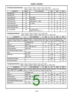
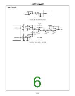
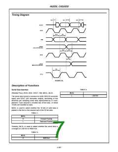
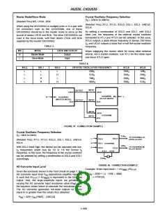
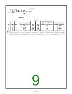
HI2555, CXD2555
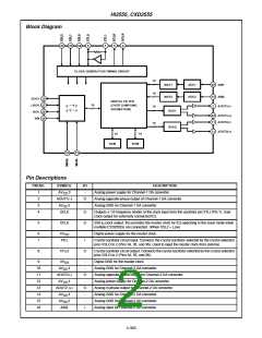
Block Diagram
36
35
34
8
7
5
4
CLOCK GENERATOR/TIMING CIRCUIT
16
16
MAF1
MAF2
ADC1
ADC2
45 AIN1
16 AIN2
SOUT 30
LRCK 27
BCK 28
SIN 29
DIGITAL FILTER
(OVER SAMPLING
DECIMATION)
16
S
S
→
←
P
P
2
AOUT1(-)
16
16
DAC1
48 AOUT1(+)
11 AOUT2(-)
DAC2
13 AOUT2(+)
16
10
RAM
ROM
32
33
Pin Descriptions
PIN NO.
SYMBOL
I/O
-
DESCRIPTION
1
2
3
4
AV
3
Analog power supply for Channel-1 DA converter.
Analog opposite-phase output of Channel-1 DA converter
Analog GND for Channel-1 DA converter.
DD
AOUT1(–)
AV
O
-
3
SS
UCLK
O
Outputs a 1/2 frequency divider of the clock input form the oscillator pin XTLI (Pin 7). User
clock output for externally connected ICs.
5
XCLK
O
256 f clock output. this provides the master clock for ICs operating in the slave mode when
S
multiple CXD255Qs are connected. (When XSL2 = Low)
6
7
XV
-
I
Digital power supply for the master clock.
DD
XTLI
Crystal oscillator circuit input. Connects the crystal oscillator selected by the crystal selection
pins XSLO to 2 (Pins 34, 35, and 36). Used to input the master clock from external.
8
XTLO
O
Crystal oscillator circuit output. Connects the crystal oscillator selected by the crystal selection
pins XSLO to 2 (Pins 34, 35, and 36).
9
XV
SS
-
-
Digital GND for the master clock.
10
11
12
12
14
15
16
AV
SS
4
Analog GND for Channel-2 DA converter.
Analog opposite-phase output for Channel-2 DA converter.
Analog power supply for Channel-2 DA converter.
Analog in-phase output for Channel-2 DA converter.
Analog GND for Channel-2 DA converter.
Analog GND for Channel-2 AD converter.
Analog input for Channel-2 AD converter.
AOUT2(-)
AV
O
-
4
DD
AOUT2 (+)
O
-
AV
AV
4
2
SS
-
SS
AIN2
I
4-302

 INTERSIL [ Intersil ]