CA3094, CA3094A, CA3094B
Test Circuits (Continued)
120VAC
R
V+ = 30V
LOAD
+15V
E
R
1
OUT
R
R
3
R
5
2
7
S
2
56kΩ
8
R
4
5
6
+
5
3
2
S
1
MT
MT
7
2
1
R
3
CA3094A
R
2
8
6
R
6
-
2
-
(NOTE 12)
D
1
CA3094A
R
1
4
R
8
3
+
C
1
R
7
OUTPUT
4
2kΩ
1
51Ω
COMMON
R
C
NOTES:
S
C
1
C
-15V
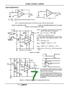
12. C = 0.5µF
1
29V
3V
D
R
R
R
R
R
R
R
R
= 1N914
1
1
2
3
4
5
6
7
8
3
6
0
0
= 0.51MΩ = 3 min.
= 5.1MΩ = 30 min.
= 22MΩ = 2 hrs.
= 44MΩ = 4 hrs.
= 1.5kΩ
= 50kΩ
= 5.1kΩ
= 1.5kΩ
27V
CLOSED
LOOP GAIN
(dB)
Time = 1 hr.
Set to R
R
R
(kΩ)
R
3
(kΩ)
1
2
S
2
4
(kΩ)
10
10
1
0
10
∞
20
40
1
10
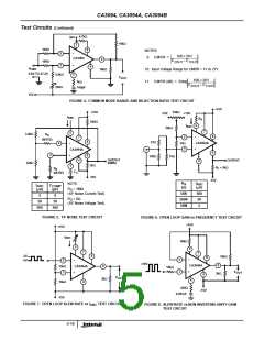
13. Potentiometer required for initial time set to permit device inter-
0.1
10
o
connecting. Time variation with temperature <0.3%/ C.
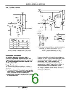
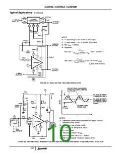
FIGURE 9. PHASE COMPENSATION TEST CIRCUIT
FIGURE 10. PRESETTABLE ANALOG TIMER
Application Information
For additional application information, refer to
Application Note AN6048, “Some Applications of a
Programmable Power/Switch Amplifier IC” and AN6077
“An IC Operational Transconductance Amplifier (OTA)
with Power Capability”.
If the desired sensitivity and required input resistance are
not known and are to be experimentally determined, or the
anticipated equipment design is sufficiently flexible to
tolerate a wide range of these parameters, it is
recommended that the equipment designer begin his
calculations with an I
characterized at this value of amplifier bias current.
of 100µA, since the CA3094 is
ABC
Design Considerations
The selection of the optimum amplifier bias current (I
depends on:
)
ABC
The CA3094 is extremely versatile and can be used in a
wide variety of applications.
1. The Desired Sensitivity - The higher the I
, the higher
ABC
the sensitivity, i.e., a greater drive current capability at the
output for a specific voltage change at the input.
2. Required Input Resistance - The lower the I
er the input resistance.
, the high-
ABC
3-17

 INTERSIL [ Intersil ]