CA3094, CA3094A, CA3094B
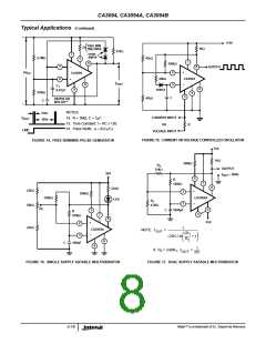
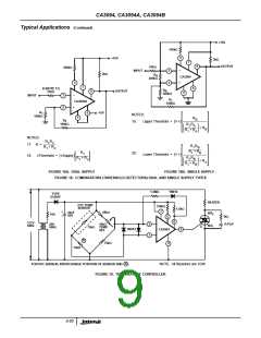
1/F Noise Measurement Circuit
Operating Considerations
When using the CA3094, A, or B audio amplifier circuits, it is
frequently necessary to consider the noise performance of the
device. Noise measurements are made in the circuit shown in
Figure 20. This circuit is a 30dB, non-inverting amplifier with
emitter follower output and phase compensation from
The “Sink” Output (Terminal 8) and the “Drive” Output
(Terminal 6) of the CA3094 are not inherently current (or
power) limited. Therefore, if a load is connected between
Terminal 6 and Terminal 4 (V- or Ground), it is important to
connect a current limiting resistor between Terminal 8 and
Terminal 7 (V+) to protect transistor Q13 under shorted load
conditions. Similarly, if a load is connected between Terminal
8 and Terminal 7 (V+), the current limiting resistor should be
connected between Terminal 6 and Terminal 4 or ground. In
circuit applications where the emitter of the output transistor
is not connected to the most negative potential in the
system, it is recommended that a 100Ω current limiting
resistor be inserted between Terminal 7 and the V+ supply.
Terminal 2 to ground. Source resistors (R ) are set to 0Ω or
S
1MΩ for E noise and I noise measurements, respectively.
These measurements are made at frequencies of 10Hz,
100Hz and 1kHz with a 1Hz measurement bandwidth. Typical
values for 1/f noise at 10Hz and 50µA I
ABC
are:
E
= 18nV ⁄ Hz and
I
= 1.8pA ⁄ Hz .
N
N
Test Circuits
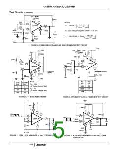
NOTES:
3. Input Offset Voltage: V
30V
E
OUT
= ----------------- .
IO
100
4. For Power Supply Rejection Test: (1) vary V+ by -2V; then (2)
300kΩ
7
vary V- by +2V.
9.9kΩ
5
5. Equations:
E OUT – E OUT
2
0
1
(1)
V+ Rejection = ------------------------------------------------
CA3094
6
200
3
1
E OUT – E OUT
0
2
10kΩ
(2)
V- Rejection = ------------------------------------------------
8
100Ω
200
1kΩ
E
OUT
4
100Ω
1
100pF
---------------------------------------------
V
6. Power Supply Rejection: (dB) = 20log
† Maximum Reading of Step 1 or Step 2
.
REJECTION†
30V
15V
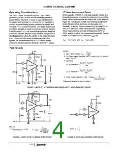
FIGURE 1. INPUT OFFSET VOLTAGE AND POWER SUPPLY REJECTION TEST CIRCUIT
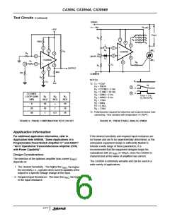
30V
30V
R
ABC
7
5
1MΩ
8
2
3
300kΩ
7
CA3094
6
5
2
3
-
1
150kΩ
CA3094A
+
E
OUT
220Ω
4
15V
1MΩ
0.001µF
4
15V
NOTES:
7. P
E
I
2
OUT
NOTE: I = --
= (V+)(I)
8. I
= -------------------------------
10
I
DISSIPATION
OS
VOLTS
--------------------
AMPS
6
FIGURE 3. INPUT BIAS CURRENT TEST CIRCUIT
FIGURE 2. INPUT OFFSET CURRENT TEST CIRCUIT
3-15

 INTERSIL [ Intersil ]