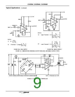
CA3094, CA3094A, CA3094B
Absolute Maximum Ratings
Thermal Information
o
o
Supply Voltage (Between V+ and V- Terminals)
Thermal Resistance (Typical, Note 2)
PDIP Package . . . . . . . . . . . . . . . . . . .
SOIC Package . . . . . . . . . . . . . . . . . . .
Metal Can Package . . . . . . . . . . . . . . .
θ
( C/W)
θ
( C/W)
JA
JC
CA3094 . . . . . . . . . . . . . . . . . . . . . . . . . . . . . . . . . . . . . . . . . 24V
CA3094A . . . . . . . . . . . . . . . . . . . . . . . . . . . . . . . . . . . . . . . . 36V
CA3094B . . . . . . . . . . . . . . . . . . . . . . . . . . . . . . . . . . . . . . . . 44V
Differential Input Voltage (Terminals 2 and 3, Note 1) . . . . . . . . . 5V
DC Input Voltage . . . . . . . . . . . . . . . . . . . . . . . . . . . . . . . . . V+ to V-
Input Current (Terminals 2 and 3) . . . . . . . . . . . . . . . . . . . . . . ±1mA
Amplifier Bias Current (Terminal 5) . . . . . . . . . . . . . . . . . . . . . . 2mA
Average Output Current. . . . . . . . . . . . . . . . . . . . . . . . . . . . . 100mA
Peak Output Current . . . . . . . . . . . . . . . . . . . . . . . . . . . . . . . 300mA
130
170
175
N/A
N/A
100
o
Maximum Junction Temperature (Metal Can Package) . . . . . . .175 C
Maximum Junction Temperature (Plastic Package) . . . . . . . .150 C
Maximum Storage Temperature Range. . . . . . . . . . -65 C to 150 C
Maximum Lead Temperature (Soldering 10s) . . . . . . . . . . . . 300 C
o
o
o
o
(SOIC - Lead Tips Only)
Operating Conditions
o
o
Temperature Range . . . . . . . . . . . . . . . . . . . . . . . . . -55 C to 125 C
CAUTION: Stresses above those listed in “Absolute Maximum Ratings” may cause permanent damage to the device. This is a stress only rating and operation of the
device at these or any other conditions above those indicated in the operational sections of this specification is not implied.
NOTES:
1. Exceeding this voltage rating will not damage the device unless the peak input signal current (1mA) is also exceeded.
2. θ is measured with the component mounted on an evaluation PC board in free air.
JA
o
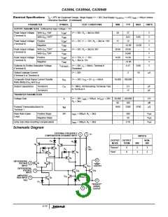
Electrical Specifications T = 25 C for Equipment Design. Single Supply V+ = 30V, Dual Supply V
= ±15V, I
= 100µA Unless
A
SUPPLY
ABC
Otherwise Specified
PARAMETER
INPUT PARAMETERS
SYMBOL
TEST CONDITIONS
MIN
TYP
MAX
UNITS
o
Input Offset Voltage
V
T = 25 C
A
-
-
-
0.4
-
5.0
7.0
8.0
mV
mV
mV
IO
o
o
T = 0 C to 70 C
A
Input Offset Voltage Change
Input Offset Current
|∆V
|
Change in V between I
IO ABC
= 100µA
1
IO
and I
= 5µA
ABC
o
I
T = 25 C
A
-
-
0.02
-
0.2
0.3
µA
µA
µA
µA
mW
dB
V
IO
o
o
T = 0 C to 70 C
A
o
Input Bias Current
I
T = 25 C
A
-
0.2
-
0.50
I
o
o
T = 0 C to 70 C
-
0.70
A
Device Dissipation
P
I
= 0mA
OUT
8
10
12
-
D
Common Mode Rejection Ratio
Common Mode Input Voltage Range
CMRR
70
27
1.0
12
-14
-
110
28.8
0.5
13.8
-14.5
30
V
V+ = 30V (High)
V- = 0V (Low)
V+ = 15V
-
ICR
-
V
-
V
V- = -15V
-
V
Unity Gain Bandwidth
f
I
I
= 7.5mA, V
= 7.5mA, V
= 15V, I
= 500µA
= 500µA
-
MHz
kHz
%
T
C
C
CE
ABC
ABC
Open Loop Bandwidth at -3dB Point
BW
OL
= 15V, I
-
4
-
CE
Total Harmonic Distortion
(Class A Operation)
THD
P
P
= 220mW
= 600mW
-
0.4
1.4
0.68
-
D
D
-
-
%
Amplifier Bias Voltage
V
-
-
V
ABC
(Terminal 5 to Terminal 4)
o
Input Offset Voltage Temperature
Coefficient
∆V /∆T
IO
-
4
-
µV/ C
Power Supply Rejection
1/F Noise Voltage
∆V /∆V
-
15
18
150
µV/V
IO
E
N
f = 10Hz, I
f = 10Hz, I
= 50µA
-
-
-
-
-
nV/ Hz
ABC
ABC
1/F Noise Current
I
= 50µA
-
0.50
-
1.8
1.0
2.6
N
pA/ Hz
Differential Input Resistance
Differential Input Capacitance
R
C
I
= 20µA
MΩ
I
I
ABC
f = 1MHz, V+ = 30V
pF
3-13

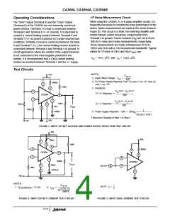
 INTERSIL [ Intersil ]