BBT3821
Electrical Characteristics
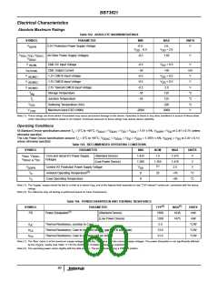
Absolute Maximum Ratings
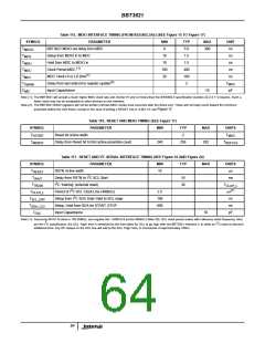
Table 102. ABSOLUTE MAXIMUM RATINGS
SYMBOL
PARAMETER
MIN
-0.5,
MAX
UNITS
V
2.5V Protection Power Supply Voltage
2.6,
V
DDPR
V
- 0.5
V
V
+ 2.0
DD
DD
V
V
DDAV
V
All Other Power Supply Voltages
-0.5
1.65
V
DDA, DD, DDAC,
V
V
CML DC Input Voltage
-0.5
- 50
-0.5
-0.5
-0.5
- 55
- 55
+ 0.5
V
mA
V
INCML
DD
+50
I
CML Output Current
OUTCML
V
1.2V CMOS Input Voltage
1.5V CMOS Input Voltage
2.5V Tolerant CMOS Input Voltage
Storage Temperature
V
V
+ 0.5
INCMS1
INCMS2
INCMS3
DD
DD
V
V
+ 0.5
V
2.6
V
T
125
125
°C
°C
°C
V
stg
T
Junction Temperature
j
T
V
Soldering Temperature (10s)
Maximum Input ESD (HBM)
220
SOL
ESD
-2000
2000
Note (1): These ratings are those which if exceeded may cause permanent damage to the device. Operation at these or any other conditions in excess of those listed
under Operating Conditions below is not implied. Continued exposure to these ratings may reduce device reliability.
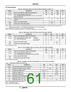
Operating Conditions
All Standard Device specifications assume T = 0°C to +85°C, V
C
= V
= V
= V
= 1.5V ± 5%, V
= V
or 2.4V ± 0.1V, unless
DD
DDAC
DDAV
DD
DDA
= V
DDPR
otherwise specified.
The Low Power Device specifications assume T = 0°C to +85°C, V
C
= V
= V
= 1.355V ± 4%, V
= V
DD
or 2.4V ± 0.1V,
DDAC
DDAV
DD
DDA
DDPR
unless otherwise specified.
Table 103. RECOMMENDED OPERATING CONDITIONS
SYMBOL
PARAMETER
MIN
NOM
MAX
UNITS
V
V
V
,
Core and Serial I/O Power Supply
Voltages
(Standard Device)
1.425
1.300
1.5
1.575
1.410
2.5
V
V
DDA DDAV
V
DDAC & DD
(Low Power Device)
1.355
(1)
V
Control I/O Protection Power Supply Voltage
V
V
DDPR
DD
0
(2)
T
Ambient Operating Temperature
25
+70
°C
°C
A
T
Case Operating Temperature
0
+85
C
Note (1): The V
supply should be tied to a level at or above V , and at the highest level expected on any “2.5V tolerant” control pin, consistent with the above
DD
DDPR
ratings.
Note (2): For reference only. All testing is performed based on Case Temperature.
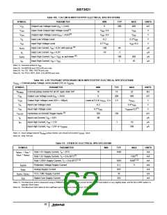
Table 104. POWER DISSIPATION AND THERMAL RESISTANCE
PARAMETER
(1)
(1)
SYMBOL
TYP
MAX
UNITS
mW
(2)
PD
Power Dissipation
(Standard Device)
1650
1350
2.0
1830
1475
(Low Power Device)
mW
θ
Thermal Resistance, Junction to Case
°C/W
°C/W
°C/W
JC
CA
CA
θ
θ
Thermal Resistance, Case to Ambient (still air, gap filler & cold plate)
Thermal Resistance, Case to Ambient (still air only)
13.0
31.0
Note (1): The ‘Max’ value is at the maximum supply voltages, while the ‘Typ’ value is at the nominal supply voltages. The power dissipation is not significantly affected
by the V supply (see Table 111 for the distribution of power between the supplies).
DDPR
Note (2): The operating power varies slightly with the data pattern. The part is tested using a PRBS23 pattern.
60

 INTERSIL [ Intersil ]