BBT3821
AC and Timing Characteristics
All specifications assume T = 0°C to +85°C, and V
= V
= V
= V
DDA
= 1.5V ± 5% (for the Standard Device) or V
= V
= V
DDAV DD
C
DDAC
DDAV DD
between V and 2.5V, unless otherwise specified.
DD
DDAC
= V
= 1.35V ± 4%(for the Low Power Device), V
DDA
DDPR
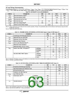
Table 112. REFERENCE CLOCK REQUIREMENTS
SYMBOL
PARAMETER
MIN
124.4
-100
TYP
MAX
159.375
+100
1.5
UNITS
MHz
ppm
ns
(1)
F
Ref clock frequency range
Ref clock frequency offset
REF
∆F
REF
T
Ref clock Rise and Fall Time
Ref clock duty cycle
REFRF
DTC
45
50
55
%
REF
REF
CM
(2)
∆V
Ref Clock Voltage Swing
300
1000
mV
V
V
Internal Common Mode Voltage
V
/2
DD
Note (1): System requirements are normally much more restrictive, typically ± 100 ppm. This specification refers to the full reference clock frequency range over which
the BBT3821 will operate.
Note (2): Single-ended peak-to-peak swing.
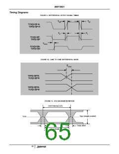
Table 113. TRANSMIT SERIAL DIFFERENTIAL OUTPUTS (SEE Figure 9, Figure 10 AND Figure 11)
SYMBOL
PARAMETER
TCXnP/N and TXPxP/N output data rate
Differential Rise time (20%-80%)
Differential Fall time (20%-80%)
MIN
2.448
60
TYP
MAX
3.1875
130
UNIT
Gbps
ps
T
110
110
TBD
15
DR
T
60
130
ps
DF
T
Differential Skew Tolerance
ps
DTOL
(2)
T
Lane to Lane Differential Skew
ps
ODS
Differential Output Impedance
100
Ω
Differential Return Loss (to 2.5GHz)
10
dB
ps
(1)
TX
RJ
Random Jitter (RMS, 1100 pattern)
2.488Gbps
3.125Gbps
3.1875
2
4.5
4.5
TBD
8
2.5
ps
TBD
ps
7
Total Jitter (RMS, PRBS pattern)
2.488Gbps
3.125Gbps
3.1875
ps
6
8
ps
8
ps
Note (1): Strictly the 1100 pattern causes a small additional non-random jitter, so that the true random jitter is slightly less than that shown.
Note (2): Parameter is guaranteed by design
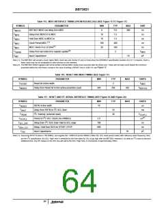
Table 114. RECEIVE SERIAL DIFFERENTIAL INPUT TIMING REQUIREMENTS (SEE Figure 11)
SYMBOL
PARAMETER
RCXnP/N & RXPnP/N Input Data Rate
MIN
2.448
-200
TYP
MAX
3.1875
+200
2500
2
UNITS
Gbps
ppm
bits
µs
Input Rate deviation from Reference Clock
Bit Synchronization Time
Frequency Lock after Power-up
Input Differential Skew
T
75
ps
DTOL
(1,2)
T
Deterministic Jitter
2.488Gbps
3.125Gbps
3.1875
TBD
0.7
UI
DJ
UI
TBD
TBD
0.88
TBD
UI
T
Total jitter tolerance
2.488Gbps
3.125Gbps
3.1875
UI
JI
UI
UI
-12
Note (1): Jitter specifications include all but 10
of the jitter population.
Note (2): Near end driven by BBT3821 Tx without pre-emphasis.
63

 INTERSIL [ Intersil ]