1-Gbit P30 Family
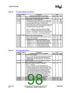
Table 38.
Protection Register Information
Offset(1)
Hex
Length
Description
P = 10Ah
(Optional flash features and commands)
Add. Code Value
(P+E)h
1
4
Number of Protection register fields in JEDEC ID space.
“00h,” indicates that 256 protection fields are available
Protection Field 1: Protection Description
This field describes user-available One Time Programmable
(OTP) Protection register bytes. Some are pre-programmed
with device-unique serial numbers. Others are user
programmable. Bits 0–15 point to the Protection register Lock
byte, the section’s first byte. The following bytes are factory
pre-programmed and user-programmable.
118: --02
2
(P+F)h
(P+10)h
(P+11)h
(P+12)h
119: --80
11A: --00
11B: --03 8 byte
11C: --03 8 byte
80h
00h
bits 0–7 = Lock/bytes Jedec-plane physical low address
bits 8–15 = Lock/bytes Jedec-plane physical high address
bits 16–23 = “n” such that 2n = factory pre-programmed bytes
bits 24–31 = “n” such that 2n = user programmable bytes
(P+13)h
(P+14)h
(P+15)h
(P+16)h
(P+17)h
(P+18)h
(P+19)h
(P+1A)h
(P+1B)h
(P+1C)h
10
Protection Field 2: Protection Description
Bits 0–31 point to the Protection register physical Lock-word
address in the Jedec-plane.
11D: --89
11E: --00
11F: --00
120: --00
89h
00h
00h
00h
0
0
0
16
0
16
Following bytes are factory or user-programmable.
∴
bits 32–39 = “n” n = factory pgm'd groups (low byte)
--00
--00
--00
121:
122:
123:
∴
bits 40–47 = “n” n = factory pgm'd groups (high byte)
bits 48–55 = “n” \ 2n = factory programmable bytes/group
∴
bits 56–63 = “n” n = user pgm'd groups (low byte)
124: --10
--00
125:
126:
∴
bits 64–71 = “n” n = user pgm'd groups (high byte)
n
∴
bits 72–79 = “n” 2 = user programmable bytes/group
--04
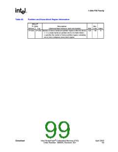
Table 39.
Burst Read Information
Offset(1)
Hex
Length
Description
P = 10Ah
(Optional flash features and commands)
Add. Code Value
(P+1D)h
1
Page Mode Read capability
127: --03 8 byte
bits 0–7 = “n” such that 2n HEX value represents the number of
read-page bytes. See offset 28h for device word width to
determine page-mode data output width. 00h indicates no
read page buffer.
Number of synchronous mode read configuration fields that
follow. 00h indicates no burst capability.
Synchronous mode read capability configuration 1
Bits 3–7 = Reserved
(P+1E)h
(P+1F)h
1
1
128: --04
129: --01
4
4
bits 0–2 “n” such that 2n+1 HEX value represents the
maximum number of continuous synchronous reads when
the device is configured for its maximum word width. A value
of 07h indicates that the device is capable of continuous
linear bursts that will output data until the internal burst
counter reaches the end of the device’s burstable address
space. This field’s 3-bit value can be written directly to the
Read Configuration Register bits 0–2 if the device is
configured for its maximum word width. See offset 28h for
word width to determine the burst data output width.
Synchronous mode read capability configuration 2
Synchronous mode read capability configuration 3
Synchronous mode read capability configuration 4
(P+20)h
(P+21)h
(P+22)h
1
1
1
12A: --02
12B: --03
12C: --07
8
16
Cont
April 2005
98
Intel StrataFlash® Embedded Memory (P30)
Order Number: 306666, Revision: 001
Datasheet

 INTEL [ INTEL ]