1-Gbit P30 Family
10.3.5
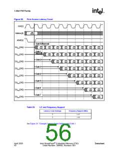
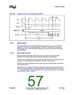
WAIT Delay
The WAIT Delay (WD) bit controls the WAIT assertion-delay behavior during synchronous burst
reads. WAIT can be asserted either during or one data cycle before valid data is output on
DQ[15:0]. When WD is set, WAIT is deasserted one data cycle before valid data (default). When
WD is cleared, WAIT is deasserted during valid data.
10.3.6
Burst Sequence
The Burst Sequence (BS) bit selects linear-burst sequence (default). Only linear-burst sequence is
supported. Table 25 shows the synchronous burst sequence for all burst lengths, as well as the
effect of the Burst Wrap (BW) setting.
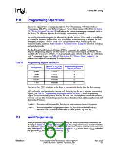
Table 25.
Burst Sequence Word Ordering
Burst Addressing Sequence (DEC)
Start
Burst Wrap
(RCR[3])
Addr.
4-Word Burst
(BL[2:0] = 0b001)
8-Word Burst
16-Word Burst
(BL[2:0] = 0b011)
Continuous Burst
(BL[2:0] = 0b111)
(DEC)
(BL[2:0] = 0b010)
0
1
2
3
4
5
6
7
0
0
0
0
0
0
0
0
0-1-2-3
1-2-3-0
2-3-0-1
3-0-1-2
0-1-2-3-4-5-6-7
1-2-3-4-5-6-7-0
2-3-4-5-6-7-0-1
3-4-5-6-7-0-1-2
4-5-6-7-0-1-2-3
5-6-7-0-1-2-3-4
6-7-0-1-2-3-4-5
7-0-1-2-3-4-5-6
0-1-2-3-4…14-15
0-1-2-3-4-5-6-…
1-2-3-4-5…15-0
1-2-3-4-5-6-7-…
2-3-4-5-6-7-8-…
3-4-5-6-7-8-9-…
4-5-6-7-8-9-10…
5-6-7-8-9-10-11…
2-3-4-5-6…15-0-1
3-4-5-6-7…15-0-1-2
4-5-6-7-8…15-0-1-2-3
5-6-7-8-9…15-0-1-2-3-4
6-7-8-9-10…15-0-1-2-3-4-5 6-7-8-9-10-11-12-…
7-8-9-10…15-0-1-2-3-4-5-6 7-8-9-10-11-12-13…
14
15
0
0
14-15-0-1-2…12-13
15-0-1-2-3…13-14
14-15-16-17-18-19-20-…
15-16-17-18-19-20-21-…
0
1
2
3
4
5
6
7
1
1
1
1
1
1
1
1
0-1-2-3
1-2-3-4
2-3-4-5
3-4-5-6
0-1-2-3-4-5-6-7
0-1-2-3-4…14-15
1-2-3-4-5…15-16
2-3-4-5-6…16-17
3-4-5-6-7…17-18
4-5-6-7-8…18-19
5-6-7-8-9…19-20
6-7-8-9-10…20-21
0-1-2-3-4-5-6-…
1-2-3-4-5-6-7-…
2-3-4-5-6-7-8-…
3-4-5-6-7-8-9-…
4-5-6-7-8-9-10…
5-6-7-8-9-10-11…
6-7-8-9-10-11-12-…
7-8-9-10-11-12-13…
1-2-3-4-5-6-7-8
2-3-4-5-6-7-8-9
3-4-5-6-7-8-9-10
4-5-6-7-8-9-10-11
5-6-7-8-9-10-11-12
6-7-8-9-10-11-12-13
7-8-9-10-11-12-13-14 7-8-9-10-11…21-22
14
15
1
1
14-15-16-17-18…28-29
15-16-17-18-19…29-30
14-15-16-17-18-19-20-…
15-16-17-18-19-20-21-…
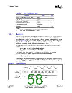
10.3.7
10.3.8
Clock Edge
The Clock Edge (CE) bit selects either a rising (default) or falling clock edge for CLK. This clock
edge is used at the start of a burst cycle, to output synchronous data, and to assert/deassert WAIT.
Burst Wrap
The Burst Wrap (BW) bit determines whether 4-word, 8-word, or 16-word burst length accesses
wrap within the selected word-length boundaries or cross word-length boundaries. When BW is
set, burst wrapping does not occur (default). When BW is cleared, burst wrapping occurs.
When performing synchronous burst reads with BW set (no wrap), an output delay may occur
when the burst sequence crosses its first device-row (16-word) boundary. If the burst sequence’s
start address is 4-word aligned, then no delay occurs. If the start address is at the end of a 4-word
Datasheet
Intel StrataFlash® Embedded Memory (P30)
Order Number: 306666, Revision: 001
April 2005
59

 INTEL [ INTEL ]