1-Gbit P30 Family
During programming, the Write State Machine (WSM) executes a sequence of internally-timed
events that program the desired data bits at the addressed location, and verifies that the bits are
sufficiently programmed. Programming the flash memory array changes “ones” to “zeros”.
Memory array bits that are zeros can be changed to ones only by erasing the block (see Section
12.0, “Erase Operations” on page 67).
The Status Register can be examined for programming progress and errors by reading at any
address. The device remains in the Read Status Register state until another command is written to
the device.
Status Register bit SR[7] indicates the programming status while the sequence executes.
Commands that can be issued to the device during programming are Program Suspend, Read Status
Register, Read Device Identifier, CFI Query, and Read Array (this returns unknown data).
When programming has finished, Status Register bit SR[4] (when set) indicates a programming
failure. If SR[3] is set, the WSM could not perform the word programming operation because VPP
was outside of its acceptable limits. If SR[1] is set, the word programming operation attempted to
program a locked block, causing the operation to abort.
Before issuing a new command, the Status Register contents should be examined and then cleared
using the Clear Status Register command. Any valid command can follow, when word
programming has completed.
11.1.1
Factory Word Programming
Factory word programming is similar to word programming in that it uses the same commands and
programming algorithms. However, factory word programming enhances the programming
performance with VPP = VPPH. This can enable faster programming times during OEM
manufacturing processes. Factory word programming is not intended for extended use. See Section
5.2, “Operating Conditions” on page 30 for limitations when VPP = VPPH
.
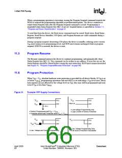
Note:
When VPP = VPPL, the device draws programming current from the VCC supply. If VPP is driven
by a logic signal, VPPL must remain above VPPL MIN to program the device. When VPP = VPPH
the device draws programming current from the VPP supply. Figure 31, “Example VPP Supply
Connections” on page 66 shows examples of device power supply configurations.
,
11.2
Buffered Programming
The device features a 32-word buffer to enable optimum programming performance. For Buffered
Programming, data is first written to an on-chip write buffer. Then the buffer data is programmed
into the flash memory array in buffer-size increments. This can improve system programming
performance significantly over non-buffered programming.
When the Buffered Programming Setup command is issued (see Section 9.2, “Device Commands”
on page 50), Status Register information is updated and reflects the availability of the buffer. SR[7]
indicates buffer availability: if set, the buffer is available; if cleared, the buffer is not available. To
retry, issue the Buffered Programming Setup command again, and re-check SR[7]. When SR[7] is
set, the buffer is ready for loading. (see Figure 42, “Buffer Program Flowchart” on page 87).
On the next write, a word count is written to the device at the buffer address. This tells the device
how many data words will be written to the buffer, up to the maximum size of the buffer.
April 2005
62
Intel StrataFlash® Embedded Memory (P30)
Order Number: 306666, Revision: 001
Datasheet

 INTEL [ INTEL ]