Timing Model & Specifications
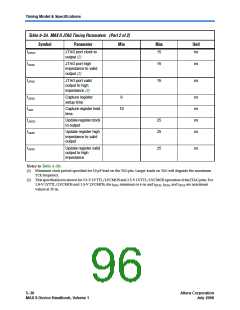
Table 5–34. MAX II JTAG Timing Parameters (Part 2 of 2)
Symbol
Parameter
Min
Max
Unit
tJPCO
JTAG port clock to
15
ns
output (2)
tJPZX
JTAG port high
impedance to valid
output (2)
15
15
ns
ns
tJPXZ
JTAG port valid
output to high
impedance (2)
tJSSU
tJSH
tJSCO
tJSZX
Capture register
setup time
8
ns
ns
ns
ns
Capture register hold
time
10
Updateregisterclock
to output
25
25
Update register high
impedance to valid
output
tJSXZ
Update register valid
output to high
25
ns
impedance
Notes to Table 5–34:
(1) Minimum clock period specified for 10 pF load on the TDOpin. Larger loads on TDOwill degrade the maximum
TCKfrequency.
(2) This specification is shown for 3.3-V LVTTL/LVCMOS and 2.5-V LVTTL/LVCMOS operation of the JTAG pins. For
1.8-V LVTTL/LVCMOS and 1.5-V LVCMOS, the tJPSU minimum is 6 ns and tJPCO, tJPZX, and tJPXZ are maximum
values at 35 ns.
5–30
Core Version a.b.c variable
Altera Corporation
July 2006
MAX II Device Handbook, Volume 1

 INTEL [ INTEL ]