DC & Switching Characteristics
JTAG Timing Specifications
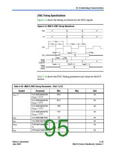
Figure 5–6 shows the timing waveforms for the JTAG signals.
Figure 5–6. MAX II JTAG Timing Waveforms
TMS
TDI
tJCP
tJCH
t JCL
tJPH
tJPSU
TCK
TDO
tJPXZ
tJPZX
tJPCO
tJSSU
tJSH
Signal
to Be
Captured
tJSCO
tJSZX
tJSXZ
Signal
to Be
Driven
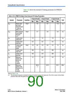
Table 5–34 shows the JTAG Timing parameters and values for MAX II
devices.
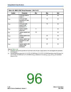
Table 5–34. MAX II JTAG Timing Parameters (Part 1 of 2)
Symbol
Parameter
Min
Max
Unit
TCKclock period for
55.5
ns
tJCP (1)
V
CCIO1 = 3.3 V
TCKclock period for
VCCIO1 = 2.5 V
62.5
100
143
ns
ns
ns
TCKclock period for
VCCIO1 = 1.8 V
TCKclock period for
V
CCIO1 = 1.5 V
tJCH
tJCL
TCKclock high time
TCKclock low time
20
20
8
ns
ns
ns
tJPSU
JTAG port setup time
(2)
tJPH
JTAG port hold time
10
ns
Altera Corporation
July 2006
Core Version a.b.c variable
5–29
MAX II Device Handbook, Volume 1

 INTEL [ INTEL ]