Chapter 1: Cyclone IV Device Datasheet
1–33
Switching Characteristics
f
For more information about the supported maximum clock rate, device and pin
planning, IP implementation, and device termination, refer to Section III: System
Performance Specifications of the External Memory Interface Handbook.
Table 1–37 lists the memory output clock jitter specifications for Cyclone IV devices.
Table 1–37. Memory Output Clock Jitter Specifications for Cyclone IV Devices (1), (2)
Parameter
Clock period jitter
Symbol
tJIT(per)
tJIT(cc)
Min
–125
–200
–150
Max
125
200
150
Unit
ps
Cycle-to-cycle period jitter
Duty cycle jitter
ps
tJIT(duty)
ps
Notes to Table 1–37:
(1) Memory output clock jitter measurements are for 200 consecutive clock cycles, as specified in the JEDEC DDR2
standard.
(2) The clock jitter specification applies to memory output clock pins generated using DDIO circuits clocked by a PLL
output routed on a global clock (GCLK) network.
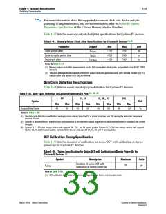
Duty Cycle Distortion Specifications
Table 1–38 lists the worst case duty cycle distortion for Cyclone IV devices.
(1), (2), (3)
Table 1–38. Duty Cycle Distortion on Cyclone IV Devices I/O Pins
C6
C7, I7
C8, I8L, A7
C9L
Symbol
Unit
Min
Max
Min
Max
Min
45
Max
Min
Max
Output Duty Cycle
45
55
45
55
55
45
55
%
Notes to Table 1–38:
(1) The duty cycle distortion specification applies to clock outputs from the PLLs, global clock tree, and IOE driving the dedicated and general
purpose I/O pins.
(2) Cyclone IV devices meet the specified duty cycle distortion at the maximum output toggle rate for each combination of I/O standard and current
strength.
(3) Cyclone IV E 1.0 V core voltage devices only support C8L, C9L, and I8L speed grades. Cyclone IV E 1.2 V core voltage devices only support
C6, C7, C8, I7, and A7 speed grades. Cyclone IV GX devices only support C6, C7, C8, and I7 speed grades.
OCT Calibration Timing Specification
Table 1–39 lists the duration of calibration for series OCT with calibration at device
power-up for Cyclone IV devices.
Table 1–39. Timing Specification for Series OCT with Calibration at Device Power-Up for
(1)
Cyclone IV Devices
Symbol
Description
Maximum
Units
Duration of series OCT with
calibration at device power-up
tOCTCAL
20
µs
Note to Table 1–39:
(1) OCT calibration takes place after device configuration and before entering user mode.
March 2016 Altera Corporation
Cyclone IV Device Handbook,
Volume 3

 INTEL [ INTEL ]