1–32
Chapter 1: Cyclone IV Device Datasheet
Switching Characteristics
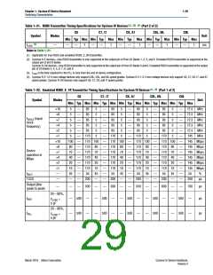
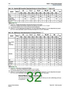
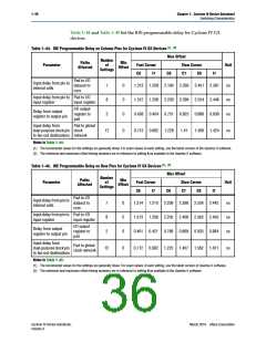
Table 1–35. Emulated LVDS Transmitter Timing Specifications for Cyclone IV Devices (1), (3) (Part 2 of 2)
C6
C7, I7
C8, A7
C8L, I8L
C9L
Symbol
tDUTY
Modes
Unit
Min
45
Max
55
Min
Max
55
Min
Max
55
Min
Max
55
Min
45
Max
55
—
—
45
—
45
—
45
—
%
TCCS
—
200
200
200
200
—
200
ps
Output jitter
(peak to peak)
—
—
500
—
500
—
550
—
—
600
1
—
—
700
1
ps
(2)
tLOCK
—
—
1
—
1
—
1
ms
Notes to Table 1–35:
(1) Cyclone IV E—emulated LVDS transmitter is supported at the output pin of all I/O Banks.
Cyclone IV GX—emulated LVDS transmitter is supported at the output pin of I/O Banks 3, 4, 5, 6, 7, 8, and 9.
(2) tLOCK is the time required for the PLL to lock from the end-of-device configuration.
(3) Cyclone IV E 1.0 V core voltage devices only support C8L, C9L, and I8L speed grades. Cyclone IV E 1.2 V core voltage devices only support
C6, C7, C8, I7, and A7 speed grades. Cyclone IV GX devices only support C6, C7, C8, and I7 speed grades.
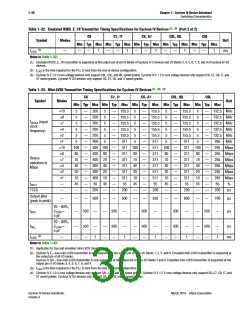
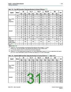
Table 1–36. LVDS Receiver Timing Specifications for Cyclone IV Devices (1), (3)
C6
C7, I7
Min
C8, A7
Min
C8L, I8L
Min
C9L
Symbol
Modes
Unit
Min
10
10
10
10
10
10
100
80
70
40
20
10
—
Max
437.5
437.5
437.5
437.5
437.5
437.5
875
Max
370
370
370
370
370
402.5
740
740
740
740
740
402.5
400
Max
320
320
320
320
320
402.5
640
640
640
640
640
402.5
400
Max
320
320
320
320
320
362
640
640
640
640
640
362
550
Min
10
10
10
10
10
10
100
80
70
40
20
10
—
Max
250
250
250
250
250
265
×10
×8
×7
×4
×2
×1
×10
×8
×7
×4
×2
×1
—
10
10
10
10
10
10
100
80
70
40
20
10
—
10
10
10
10
10
10
100
80
70
40
20
10
—
10
10
10
10
10
10
100
80
70
40
20
10
—
MHz
MHz
MHz
MHz
MHz
MHz
f
HSCLK (input
clock
frequency)
500 Mbps
500 Mbps
500 Mbps
500 Mbps
500 Mbps
265 Mbps
875
875
HSIODR
SW
875
875
437.5
400
640
700
1
ps
Input jitter
tolerance
—
—
500
—
500
—
550
—
—
600
1
—
—
ps
(2)
tLOCK
—
—
1
—
1
—
1
ms
Notes to Table 1–36:
(1) Cyclone IV E—LVDS receiver is supported at all I/O Banks.
Cyclone IV GX—LVDS receiver is supported at I/O Banks 3, 4, 5, 6, 7, 8, and 9.
(2) tLOCK is the time required for the PLL to lock from the end-of-device configuration.
(3) Cyclone IV E 1.0 V core voltage devices only support C8L, C9L, and I8L speed grades. Cyclone IV E 1.2 V core voltage devices only support
C6, C7, C8, I7, and A7 speed grades. Cyclone IV GX devices only support C6, C7, C8, and I7 speed grades.
External Memory Interface Specifications
The external memory interfaces for Cyclone IV devices are auto-calibrating and easy
to implement.
Cyclone IV Device Handbook,
Volume 3
March 2016 Altera Corporation

 INTEL [ INTEL ]