Chapter 1: Cyclone IV Device Datasheet
1–37
I/O Timing
I/O Timing
Use the following methods to determine I/O timing:
■
the Excel-based I/O Timing
the Quartus II timing analyzer
■
The Excel-based I/O timing provides pin timing performance for each device density
and speed grade. The data is typically used prior to designing the FPGA to get a
timing budget estimation as part of the link timing analysis. The Quartus II timing
analyzer provides a more accurate and precise I/O timing data based on the specifics
of the design after place-and-route is complete.
f
The Excel-based I/O Timing spreadsheet is downloadable from Cyclone IV Devices
Literature website.
Glossary
Table 1–46 lists the glossary for this chapter.
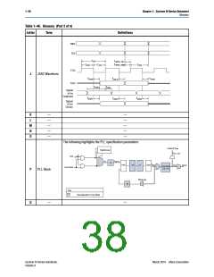
Table 1–46. Glossary (Part 1 of 5)
Letter
Term
—
Definitions
A
B
C
D
E
—
—
—
—
—
—
—
—
—
F
fHSCLK
GCLK
High-speed I/O block: High-speed receiver/transmitter input and output clock frequency.
Input pin directly to Global Clock network.
G
H
GCLK PLL
HSIODR
Input pin to Global Clock network through the PLL.
High-speed I/O block: Maximum/minimum LVDS data transfer rate (HSIODR = 1/TUI).
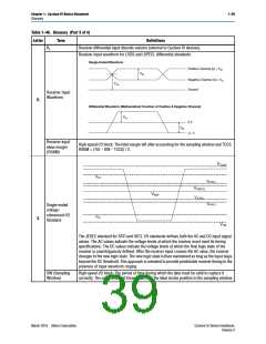
VIH
Input Waveforms
for the SSTL
Differential I/O
Standard
I
VSWING
VREF
VIL
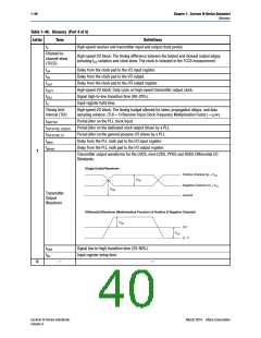
March 2016 Altera Corporation
Cyclone IV Device Handbook,
Volume 3

 INTEL [ INTEL ]