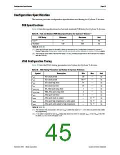
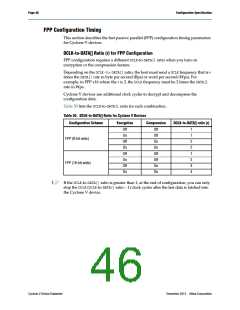
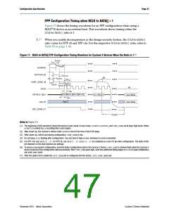
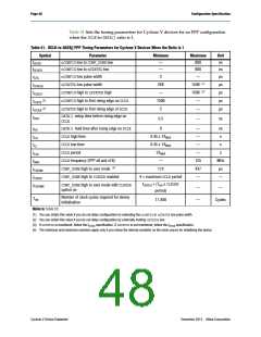
Page 44
Switching Characteristics
Figure 16 shows the timing diagram for NAND data read timing characteristics.
Figure 16. NAND Data Read Timing Diagram
Tcea
NAND_CE
Trr
Trp
Treh
NAND_RE
Trhz
NAND_RB
Trea
NAND_DQ[7:0]
Dout
ARM Trace Timing Characteristics
Table 47 lists the ARM trace timing characteristics for Cyclone V devices.
Most debugging tools have a mechanism to adjust the capture point of trace data.
Table 47. ARM Trace Timing Requirements for Cyclone V Devices
Description
Min
12.5
45
Max
—
55
1
Unit
ns
CLK clock period
CLK maximum duty cycle
%
CLK to D0 –D7 output data delay
–1
ns
UART Interface
The maximum UART baud rate is 6.25 megasymbols per second.
GPIO Interface
The minimum detectable general-purpose I/O (GPIO) pulse width is 2 µs. The pulse
width is based on a debounce clock frequency of 1 MHz.
CAN Interface
The maximum controller area network (CAN) data rate is 1 Mbps.
Cyclone V Device Datasheet
December 2013 Altera Corporation

 INTEL [ INTEL ]