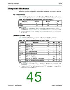
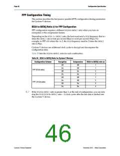
Page 42
Switching Characteristics
Table 46. NAND ONFI 1.0 Timing Requirements for Cyclone V Devices (Part 2 of 2)
Symbol
(1)
Description
Chip enable to write enable hold time
Address latch enable to write enable setup time
Address latch enable to write enable hold time
Data to write enable setup time
Min
5
Max
Unit
ns
ns
ns
ns
ns
ns
ns
ns
ns
Tceh
—
—
—
—
—
25
16
100
—
(1)
Talesu
10
5
(1)
Taleh
(1)
Tdsu
10
5
(1)
Tdh
Tcea
Trea
Trhz
Trr
Data to write enable hold time
Chip enable to data access time
—
—
—
20
Read enable to data access time
Read enable to data high impedance
Ready to read enable low
Note to Table 46:
(1) Timing of the NAND interface is controlled through the NAND Configuration registers.
Figure 13 shows the timing diagram for NAND command latch timing characteristics.
Figure 13. NAND Command Latch Timing Diagram
NAND_CLE
NAND_CE
Tclesu
Tcesu
Tcleh
Twp
Tceh
NAND_WE
NAND_ALE
Talesu
Taleh
Tdsu
Command
Tdh
NAND_DQ[7:0]
Cyclone V Device Datasheet
December 2013 Altera Corporation

 INTEL [ INTEL ]