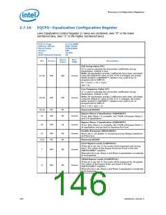
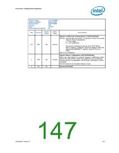
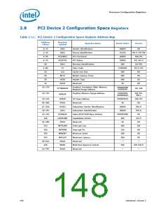
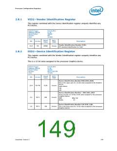
Processor Configuration Registers
2.8.3
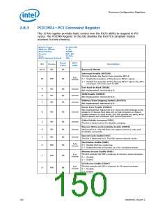
PCICMD2—PCI Command Register
This 16-bit register provides basic control over the IGD's ability to respond to PCI
cycles. The PCICMD Register in the IGD disables the IGD PCI compliant master
accesses to main memory.
B/D/F/Type:
Address Offset:
Reset Value:
Access:
0/2/0/PCI
4–5h
0000h
RW, RO
16 bits
00h
Size:
BIOS Optimal Default
Reset
Value
RST/
PWR
Bit
Access
Description
15:11
RO
0h
Reserved (RSVD)
Interrupt Disable (INTDIS)
This bit disables the device from asserting INTx#.
0 = Enable the assertion of this device's INTx# signal.
FLR,
Uncore
10
RW
0b
1 = Disable the assertion of this device's INTx# signal. DO_INTx
messages will not be sent to DMI.
Fast Back-to-Back (FB2B)
Not Implemented. Hardwired to 0.
9
8
7
RO
RO
RO
0b
0b
0b
Uncore
Uncore
Uncore
SERR Enable (SERRE)
Not Implemented. Hardwired to 0.
Address/Data Stepping Enable (ADSTEP)
Not Implemented. Hardwired to 0.
Parity Error Enable (PERRE)
Not Implemented. Hardwired to 0. Since the IGD belongs to the
category of devices that does not corrupt programs or data in
system memory or hard drives, the IGD ignores any parity error
that it detects and continues with normal operation.
6
RO
0b
Uncore
Video Palette Snooping (VPS)
This bit is hardwired to 0 to disable snooping.
5
4
3
RO
RO
RO
0b
0b
0b
Uncore
Uncore
Uncore
Memory Write and Invalidate Enable (MWIE)
Hardwired to 0. The IGD does not support memory write and
invalidate commands.
Special Cycle Enable (SCE)
This bit is hardwired to 0. The IGD ignores Special cycles.
Bus Master Enable (BME)
0 = Disable IGD bus mastering.
1 = Enable the IGD to function as a PCI compliant master.
FLR,
Uncore
2
1
RW
RW
0b
0b
Memory Access Enable (MAE)
This bit controls the IGD's response to memory space accesses.
0 = Disable.
1 = Enable.
FLR,
Uncore
I/O Access Enable (IOAE)
This bit controls the IGD's response to I/O space accesses.
0 = Disable.
1 = Enable.
FLR,
Uncore
0
RW
0b
150
Datasheet, Volume 2

 INTEL [ INTEL ]