Processor Configuration Registers
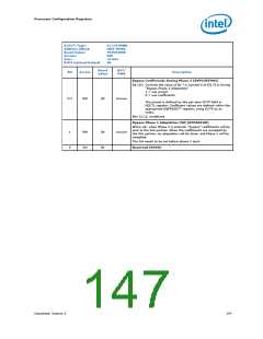
B/D/F/Type:
Address Offset:
Reset Value:
Access:
0/1/0/MMR
DD8–DDBh
F9404400h
RW
Size:
32 bits
BIOS Optimal Default
0h
Reset
Value
RST/
PWR
Bit
Access
Description
Bypass Coefficients During Phase 3 (BYPCOEFPH3)
Bit [0]: Controls the value of bit 7 in Symbol 6 of EQ TS1s during
"Bypass Phase 3 Adaptation"
1 = use preset
0 = use coefficients
5:2
RW
0h
Uncore
The preset is defined by the per-lane DCTP field in
EQCTL register. Coefficient values are defined within the
appropriate EQPRESET* register, using DCTP as an
index.
Bits [3:1]: Undefined
Bypass Phase 3 Adaptation FSM (BYPADFSM)
When set, when Phase 3 is entered, “bypass” coefficients will be
sent to the link partner. When the coefficients are accepted by
the link partner, no adaptation will be done, and Phase 3 will be
complete.
1
0
RW
RO
0b
0h
Uncore
This bit needs to be set before phase 3 start.
Reserved (RSVD)
Datasheet, Volume 2
147

 INTEL [ INTEL ]