Processor Configuration Registers
2.8
PCI Device 2 Configuration Space Registers
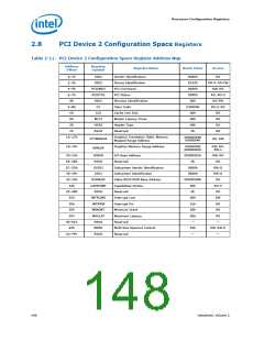
Table 2-11. PCI Device 2 Configuration Space Register Address Map
Address
Offset
Register
Symbol
Register Name
Reset Value
Access
0–1h
2–3h
4–5h
6–7h
8h
VID2
DID2
Vendor Identification
8086h
0152h
0000h
0090h
00h
RO
RO-V, RO-FW
RW, RO
RO, RO-V
RO-FW
RO-V, RO
RO
Device Identification
PCI Command
PCI Status
PCICMD2
PCISTS2
RID2
Revision Identification
Class Code
9–Bh
Ch
CC
030000h
00h
CLS
Cache Line Size
Master Latency Timer
Header Type
Dh
MLT2
00h
RO
Eh
HDR2
RSVD
00h
RO
Fh
Reserved
0h
RO
10–17h
Graphics Translation Table, Memory
Mapped Range Address
000000000
0000004h
GTTMMADR
GMADR
RO, RW
18–1Fh
Graphics Memory Range Address
00000000
0000000Ch
RW, RO,
RW-L
20–23h
24–2Bh
2C–2Dh
2E–2Fh
30–33h
34h
IOBAR
RSVD
I/O Base Address
Reserved
00000001h
0h
RW, RO
RO
SVID2
Subsystem Vendor Identification
Subsystem Identification
Video BIOS ROM Base Address
Capabilities Pointer
Reserved
0000h
0000h
00000000h
90h
RW-O
RW-O
RO
SID2
ROMADR
CAPPOINT
RSVD
RO-V
RO
35–3Bh
3Ch
0h
INTRLINE
INTRPIN
MINGNT
MAXLAT
RSVD
Interrupt Line
00h
RW
3Dh
Interrupt Pin
01h
RO
3Eh
Minimum Grant
00h
RO
3Fh
Maximum Latency
Reserved
00h
RO
40–61h
62h
—
—
MSAC
Multi Size Aperture Control
Reserved
02h
RW, RW-K
—
63–FFh
RSVD
—
148
Datasheet, Volume 2

 INTEL [ INTEL ]