Processor Configuration Registers
2.7.16
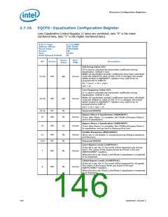
EQCFG—Equalization Configuration Register
Lane Equalization Control Register (2 lanes are combined, lane "0" is the lower
numbered lane, lane "1" is the higher numbered lane).
B/D/F/Type:
Address Offset:
Reset Value:
Access:
0/1/0/MMR
DD8–DDBh
F9404400h
RW
32 bits
0h
Size:
BIOS Optimal Default
Reset
Value
RST/
PWR
Bit
Access
Description
Full Swing Value (FS)
FS is used to calculate the transmitter coefficients during
Equalization. Default is 62d.
Note: all equalization presets’ coefficients have been calculated
using the default FS value of 62d. If FS is changed, the preset
tables located in EQPRESET* registers may need to be re-
programmed to fulfill FS.
31:26
RW
3Eh
Uncore
FS = |Cm1| + C0 + |Cp1|
(C0 > 0)
Low Frequency Value (LF)
LF is used to calculate the transmitter coefficients during
Equalization. Default is 20d.
Note: All equalization presets’ coefficients have been calculated
using the default LF value of 20d. If LF is changed, the preset
tables located in EQPRESET* registers may need to be re-
programmed to fulfill LF.
25:20
RW
14h
Uncore
Cm1 + C0 + Cp1 > LF
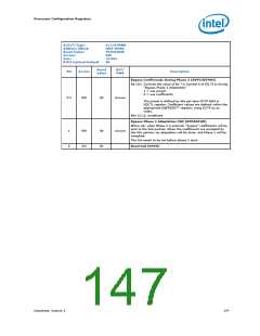
19:16
15
RO
0h
0b
Reserved (RSVD)
Bypass Phase 2 Equalization (EQPH2BYP)
If set, after Phase 1 is complete, the LTSSM will bypass Phase 2
and 3 of equalization.
RW
Uncore
Uncore
Uncore
Bypass Phase 3 Equalization (EQPH3BYP)
If set, after Phase 2 is complete, the LTSSM will bypass Phase 3
of equalization and go back to Recovery.RcvrLock.
14
RW
1b
Disable Margining (MARGINDIS)
When set, it will disable Tx margining during Polling.Compliance
and Recovery.
13
RW
RO
0b
0h
12:8
Reserved (RSVD)
Gen3 Bypass Levels (G3BYPLVL)
If this bit is set, the Tx Eq Levels will be bypassed only during
Gen3. The values of the bypass levels are found in the port
EQBYPLVLBND* registers.
When this bit is set, Phase 2 and Phase 3 equalization is expected
to be bypassed.
7
6
RW
RW
0b
0b
Uncore
Uncore
Global Bypass Levels (GLBBYPLVL)
If this bit is set, the Tx Eq Levels will be bypassed for all speeds.
The values of the bypass levels are found in the port
EQBYPLVLBND* registers.
When this bit is set, Phase 2 and Phase 3 equalization is expected
to be bypassed.
146
Datasheet, Volume 2

 INTEL [ INTEL ]