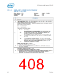
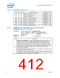
LPC Interface Bridge Registers (D31:F0)
13.1.31 BIOS_CNTL—BIOS Control Register
(LPC I/F—D31:F0)
Offset Address: DCh
Attribute:
R/WLO, R/W, RO
8 bit
Core
Default Value:
Lockable:
00h
No
Size:
Power Well:
Bit
Description
7:5
4
Reserved
Top Swap Status (TSS) — RO. This bit provides a read-only path to view the state of
the Top Swap bit that is at offset 3414h, bit 0.
SPI Read Configuration (SRC) — R/W. This 2-bit field controls two policies related to
BIOS reads on the SPI interface:
Bit 3 = Prefetch Enable
Bit 2 = Cache Disable
Settings are summarized below:
Bits 3:2
Description
No prefetching, but caching enabled. 64B demand reads load
the read buffer cache with “valid” data, allowing repeated code
fetches to the same line to complete quickly
00b
3:2
No prefetching and no caching. One-to-one correspondence of
host BIOS reads to SPI cycles. This value can be used to invalidate
the cache.
01b
Prefetching and Caching enabled. This mode is used for long
sequences of short reads to consecutive addresses (i.e., shadowing).
10b
11b
Reserved. This is an invalid configuration, caching must be
enabled when prefetching is enabled.
BIOS Lock Enable (BLE) — R/WLO.
0 = Setting the BIOSWE will not cause SMIs.
1 = Enables setting the BIOSWE bit to cause SMIs. Once set, this bit can only be
cleared by a PLTRST#.
1
0
BIOS Write Enable (BIOSWE) — R/W.
0 = Only read cycles result in Firmware Hub I/F cycles.
1 = Access to the BIOS space is enabled for both read and write cycles. When this bit is
written from a 0 to a 1 and BIOS Lock Enable (BLE) is also set, an SMI# is
generated. This ensures that only SMI code can update BIOS.
408
Datasheet

 INTEL [ INTEL ]