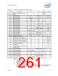
Electrical Characteristics
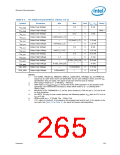
Table 8-7.
Symbol
DC Output Characteristics (Sheet 2 of 2)
Parameter
Min
Max
Unit
IOL / IOH
Notes
Output Low Voltage
Output High Voltage
Output Low Voltage
Output High Voltage
Output Low Voltage
Output High Voltage
Output Low Voltage
Output High Voltage
Output Low Voltage
Output High Voltage
Output Low Voltage
Output High Voltage
Output Low Voltage
Output High Voltage
—
0.4
V
5 mA
VOL_PWM
VOH_PWM
VOL_CL1
VOH_CL1
VOL_CL2
VOH_CL2
VOL_CL3
VOH_CL3
VOL_SST
VOH_SST
VOL_PECI
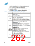
—
—
Note 1
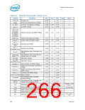
—
0.15
V
V
V
V
V
V
V
V
V
1 mA
0.485(VccCL1_5)
—
—
0.1(VccCL1_5)
1.5 mA
-1.5 mA
6 mA
0.9(VccCL1_5)
—
—
0.4
VccCL3_3 -0.5
—
-0.5 mA
0.5 mA
-6 mA
—
0.3
1.1
—
—
0.75(V_CPU_IO)
—
0.25(V_CPU_IO)
0.5 mA
-6 mA
—
0.1(VccHDA)
—
VOH_PECI
VOL_HDA
V
V
1.5 mA
-0.5 mA
VOH_HDA
0.9(VccHDA)
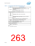
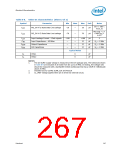
NOTES:
1.
The SERR#, PIRQ[H:A], SMBDATA, SMBCLK, LINKALERT#, SMLINK[1:0], and PWM[2:0]
signal has an open-drain driver and SATALED# has an open-collector driver, and the VOH
specification does not apply. This signal must have external pull up resistor.
PCI Express mVdiff p-p = 2*|PETp[x] – PETn[x]|
SATA Vdiff, tx (VOMIN7/VOMAX7) is measured at the SATA connector on the transmit side
(generally, the motherboard connector), where SATA mVdiff p-p = 2*|SATA[x]TXP –
SATA[x]TXN|
2.
3.
4.
5.
Maximum Iol for CPUPWRGD is 12 mA for short durations (<500 mS per 1.5 s) and 9 mA
for long durations.
For INIT3_3V only, for low current devices, the following applies: VOL5 Max is 0.15 V at an
I
OL5 of 2 mA.
6.
7.
GLAN mVdiff p-p = 2*|GLAN_TXp – GLAN_TXn|
3.3 V refers to VccSus3_3 for signals in the suspend well and to Vcc3_3 for signals in the
core well. See Table 3-2 or Table 3-3 for signal and power well association.
Datasheet
265

 INTEL [ INTEL ]