GMCH Register Description
Host-PCI Express bridge, the GMCH will generate a Type 1 Configuration Cycle TLP on
DMI.
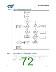
The ICH8 routes configurations accesses in a manner similar to the GMCH. The ICH8
decodes the configuration TLP and generates a corresponding configuration access.
Accesses targeting a device on PCI Bus 0 may be claimed by an internal device. The
ICH7 compares the non-zero Bus Number with the Secondary Bus Number and
Subordinate Bus Number registers of its P2P bridges to determine if the configuration
access is meant for Primary PCI, or some other downstream PCI bus or PCI Express
link.
Configuration accesses that are forwarded to the ICH8, but remain unclaimed by any
device or bridge will result in a master abort.
4.5
I/O Mapped Registers
The GMCH contains two registers that reside in the processor I/O address space − the
Configuration Address (CONFIG_ADDRESS) Register and the Configuration Data
(CONFIG_DATA) Register. The Configuration Address Register enables/disables the
configuration space and determines what portion of configuration space is visible
through the Configuration Data window.
4.5.1
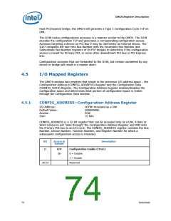
CONFIG_ADDRESS—Configuration Address Register
I/O Address:
Default Value:
Access:
0CF8h Accessed as a DW
00000000h
R/W
Size:
32 bits
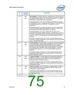
CONFIG_ADDRESS is a 32-bit register that can be accessed only as a DW. A Byte or
Word reference will "pass through" the Configuration Address Register and DMI onto
the Primary PCI bus as an I/O cycle. The CONFIG_ADDRESS register contains the Bus
Number, Device Number, Function Number, and Register Number for which a
subsequent configuration access is intended.
Bit
Access &
Default
Description
31
R/W
0b
Configuration Enable (CFGE):
0 = Disable
1 = Enable
Reserved
30:24
74
Datasheet

 INTEL [ INTEL ]