Electrical Specifications
2.6.3.1
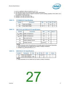
GTL+ Front Side Bus Specifications
In most cases, termination resistors are not required as these are integrated into the
processor silicon. See Table 8 for details on which GTL+ signals do not include on-die
termination.
Valid high and low levels are determined by the input buffers by comparing with a
reference voltage called GTLREF. Table 16 lists the GTLREF specifications. The GTL+
Reference voltage (GTLREF) should be generated on the system board using high
precision voltage divider circuits.
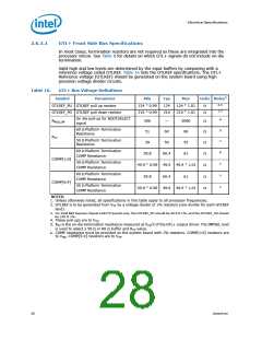
Table 16.
GTL+ Bus Voltage Definitions
Symbol
Parameter
Min
Typ
Max
Units Notes1
2,3
GTLREF_PU GTLREF pull up resistor
GTLREF_PD GTLREF pull down resistor
124 * 0.99
210 * 0.99
124
210
124 * 1.01
210 * 1.01
Ω
2,3
Ω
On die pull-up for BOOTSELECT
4
RPULLUP
signal
500
51
—
60
5000
66
Ω
60 Ω Platform Termination
Resistance
5
Ω
RTT
50 Ω Platform Termination
Resistance
5
39
50
55
Ω
60 Ω Platform Termination
6
59.8
60.4
61
Ω
COMP Resistance
COMP[1:0]
50 Ω Platform Termination
6
49.9 * 0.99
59.8
49.9
60.4
49.9
49.9 * 1.01
61
Ω
COMP Resistance
60 Ω Platform Termination
6
Ω
COMP Resistance
COMP[5:4]
50 Ω Platform Termination
6
49.9 * 0.99
49.9 * 1.01
Ω
COMP Resistance
NOTES:
1. Unless otherwise noted, all specifications in this table apply to all processor frequencies.
2. GTLREF is to be generated from VTT by a voltage divider of 1% resistors (one divider for each GTLREF
land).
3. For Intel 865 Express chipset LGA775 boards only, the GTLREF_PU should be 49.9 Ω 1%, and the GTLREF_PD should
be 100 Ω 1%.
4. These pull-ups are to VTT.
5. RTT is the on-die termination resistance measured at VTT/2 of the GTL+ output driver. The IMPSEL land
is used to select a 50 Ω or 60 Ω buffer and RTT value.
6. COMP resistance must be provided on the system board with 1% resistors. COMP[1:0] resistors are
to VSS. COMP[5:4] resistors are to VTT.
28
Datasheet

 INTEL [ INTEL ]