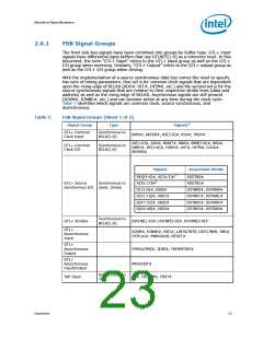
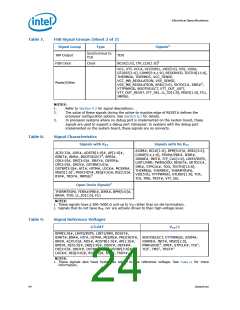
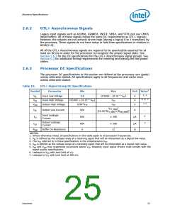
Electrical Specifications
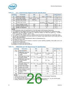
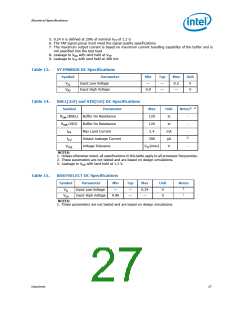
5. 0.24 V is defined at 20% of nominal VTT of 1.2 V.
6. The TAP signal group must meet the signal quality specifications.
7. The maximum output current is based on maximum current handling capability of the buffer and is
not specified into the test load.
8. Leakage to VSS with land held at VTT.
9. Leakage to VTT with land held at 300 mV.
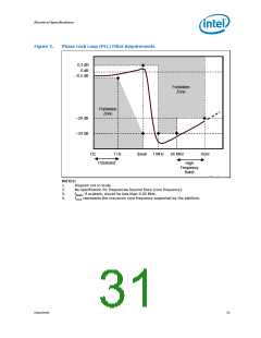
Table 13.
VTTPWRGD DC Specifications
Symbol
Parameter
Input Low Voltage
Input High Voltage
Min
Typ
Max
Unit
VIL
—
—
—
0.3
—
V
V
VIH
0.9
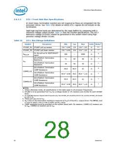
Table 14.
BSEL[2:0] and VID[5:0] DC Specifications
Symbol
Parameter
Max
Unit
Ω
Notes1, 2
R
ON (BSEL) Buffer On Resistance
120
120
-
-
RON (VID)
IOL
ILO
Buffer On Resistance
Max Land Current
Ω
2.4
mA
µA
V
-
3
Output Leakage Current
Voltage Tolerance
200
VTOL
VTT(max)
-
NOTES:
1. Unless otherwise noted, all specifications in this table apply to all processor frequencies.
2. These parameters are not tested and are based on design simulations.
3. Leakage to VSS with land held at 1.2 V.
Table 15.
BOOTSELECT DC Specifications
Symbol
Parameter
Min
Typ
Max
Unit
Notes
1
VIL
VIH
Input Low Voltage
Input High Voltage
—
—
—
0.24
—
V
V
1
0.96
NOTES:
1. These parameters are not tested and are based on design simulations.
Datasheet
27

 INTEL [ INTEL ]