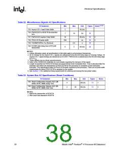
Electrical Specifications
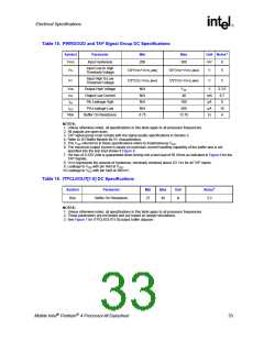
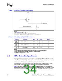
Figure 7. ITPCLKOUT[1:0] Output Buffer Diagram
Vcc
Ron
To Debug Port
Processor Package
Rext
NOTES:
1. See Table 16 for range of Ron.
2. The Vcc referred to in this figure is the instantaneous Vcc.
3. Refer to the appropriate platform design guidelines for the value of Rext.
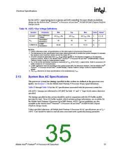
Table 17. BSEL [1:0] and VID[4:0] DC Specifications
Symbol
Parameter
Min
Max
Unit
Notes1
Ron
(BSEL)
Buffer On Resistance
9.2
14.3
Ω
2
Ron
(VID)
Buffer On Resistance
Pin Leakage Hi
7.8
12.8
100
Ω
2
3
IHI
N/A
µA
NOTES:
1. Unless otherwise noted, all specifications in this table apply to all processor frequencies.
2. These parameters are not tested and are based on design simulations.
3. Leakage to Vss with pin held at 2.50 V.
2.12
AGTL+ System Bus Specifications
Routing topology recommendations may be found in the Mobile Intel Pentium 4 Processor-M
and Intel 845MP/845MZ Chipset Platform Design Guide. Termination resistors are not required
for most AGTL+ signals, as these are integrated into the processor silicon.
Valid high and low levels are determined by the input buffers which compare a signal’s voltage
with a reference voltage called GTLREF (known as V
in previous documentation).
REF
Table 18 lists the GTLREF specifications. The AGTL+ reference voltage (GTLREF) should be
generated on the system board using high precision voltage divider circuits. It is important that the
system board impedance is held to the specified tolerance, and that the intrinsic trace capacitance
34
Mobile Intel Pentium 4 Processor-M Datasheet

 INTEL [ INTEL ]