XMC4500
XMC4000 Family
Electrical Parameters
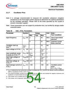
3.2.7
Oscillator Pins
Note: It is strongly recommended to measure the oscillation allowance (negative
resistance) in the final target system (layout) to determine the optimal parameters
for the oscillator operation. Please refer to the limits specified by the crystal or
ceramic resonator supplier.
Note: These parameters are not subject to production test, but verified by design and/or
characterization.
Table 28
OSC_XTAL Parameters
Parameter
Symbol
Min.
Values
Typ.
−
Unit Note /
Test Condition
Max.
Input frequency
f
OSC SR
4
4
−
40
MHz Direct Input Mode
selected
−
−
−
−
−
−
−
25
10
MHz External Crystal
Mode selected
Oscillator start-up
time1)2)
tOSCS
ms
CC
Input voltage at XTAL1 VIX SR -0.5
VDDP
0.5
+
+
+
V
Input amplitude (peak-
to-peak) at XTAL12)3)
V
V
V
PPX SR 0.4 ×
VDDP
1.0
V
VDDP
Input high voltage at
XTAL14)
IHBXSR 1.0
ILBX SR -0.5
VDDP
0.5
V
Input low voltage at
XTAL14)
0.4
V
Input leakage current at IILX1 CC -100
XTAL1
100
nA
Oscillator power
down
0 V ≤ VIX ≤ VDDP
1)
t
OSCS is defined from the moment the oscillator is enabled wih SCU_OSCHPCTRL.MODE until the oscillations
reach an amplitude at XTAL1 of 0.4 * VDDP
.
2) The external oscillator circuitry must be optimized by the customer and checked for negative resistance and
amplitude as recommended and specified by crystal suppliers.
3) If the shaper unit is enabled and not bypassed.
4) If the shaper unit is bypassed, dedicated DC-thresholds have to be met.
Data Sheet
54
V1.0, 2013-01
Subject to Agreement on the Use of Product Information

 INFINEON [ Infineon ]