XMC4500
XMC4000 Family
Electrical Parameters
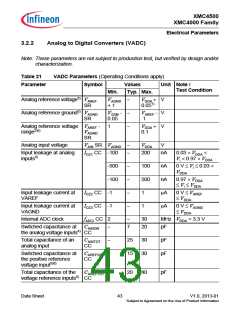
Table 21
VADC Parameters (Operating Conditions apply) (cont’d)
Parameter
Symbol
Values
Unit Note /
Test Condition
Min.
TUE CC -4
Typ. Max.
Total Unadjusted Error
−
−
4
3
LSB 12-bit resolution;
V
DDA = 3.3 V;
Differential Non-Linearity EADNL
-3
LSB
7)
Error8)
CC
VAREF = VDDA
Gain Error8)
EAGAIN
-4
−
4
LSB
CC
Integral Non-Linearity8)
Offset Error8)
EAINLCC -3
−
−
3
4
LSB
LSB
EAOFF
-4
CC
Worst case ADC VDDA
power supply current per CC
active converter
IDDAA
−
1.5
30
2
mA during conversion
VDDP = 3.6 V,
TJ = 150 oC
Charge consumption on
AREF per conversion5)
QCONV
CC
AIN CC
−
−
pC
0 V ≤ VAREF
9)
V
≤ VDDA
ON resistance of the
analog input path
R
−
700 1 700 Ohm
550 900 Ohm
700 1 700 Ohm
ON resistance for the ADC RAIN7T
test (pull down for AIN7)
180
−
CC
Resistance of the
reference voltage input
path
RAREF
CC
1) A running conversion may become imprecise in case the normal conditions are violated (voltage overshoot).
2) If the analog reference voltage is below VDDA, then the ADC converter errors increase. If the reference voltage
is reduced by the factor k (k<1), TUE, DNL, INL, Gain, and Offset errors increase also by the factor 1/k.
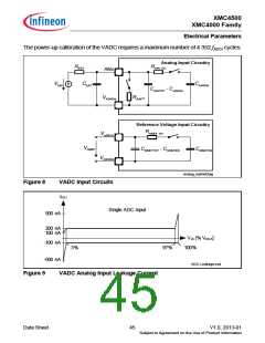
3) The leakage current definition is a continuous function, as shown in figure ADCx Analog Inputs Leakage. The
numerical values defined determine the characteristic points of the given continuous linear approximation -
they do not define step function (see Figure 9).
4) The sampling capacity of the conversion C-network is pre-charged to VAREF/2 before the sampling moment.
Because of the parasitic elements, the voltage measured at AINx can deviate from VAREF/2.
5) Applies to AINx, when used as alternate reference input.
6) This represents an equivalent switched capacitance. This capacitance is not switched to the reference voltage
at once. Instead, smaller capacitances are successively switched to the reference voltage.
7) For 10-bit conversions, the errors are reduced to 1/4; for 8-bit conversions, the errors are reduced to 1/16.
Never less than ±1 LSB.
8) The sum of DNL/INL/GAIN/OFF errors does not exceed the related total unadjusted error TUE.
9) The resulting current for a conversion can be calculated with IAREF = QCONV / tc.
The fastest 12-bit post-calibrated conversion of tc = 550 ns results in a typical average current of
I
AREF = 54.5 µA.
Data Sheet
44
V1.0, 2013-01
Subject to Agreement on the Use of Product Information

 INFINEON [ Infineon ]