XMC4500
XMC4000 Family
Electrical Parameters
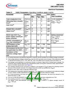
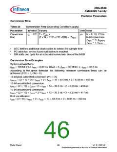
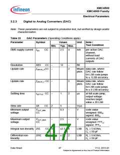
Table 23
DAC Parameters (Operating Conditions apply) (cont’d)
Parameter
Symbol
Values
Typ. Max.
±20
Unit
Note /
Test Condition
Min.
Offset error
Gain error
EDOFF CC
mV
%
EDG_IN CC -6.5
STARTUP CC −
-1.5
15
3
Startup time
t
30
μs
time from output
enabling till code
valid ±16 LSB
3dB Bandwidth of
Output Buffer
fC1
CC 2.5
5
−
−
−
MHz verified by design
Output sourcing
current
IOUT_SOURCE
CC
−
−
-30
0.6
mA
mA
Output sinking
current
IOUT_SINK
CC
Output resistance
Load resistance
Load capacitance
ROUT CC
−
5
−
−
50
−
−
Ohm
kOhm
pF
RL
CL
SR
SR
−
−
50
−
Signal-to-Noise
Ratio
SNR CC
THD CC
PSRR CC
70
dB
dB
dB
examination
bandwidth < 25 kHz
Total Harmonic
Distortion
−
−
70
56
−
−
examination
bandwidth < 25 kHz
Power Supply
Rejection Ratio
to VDDA
verified by design
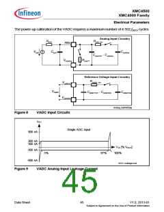
Conversion Calculation
Unsigned:
DACxDATA = 4095 × (VOUT - VOUT_MIN) / (VOUT_MAX - VOUT_MIN
)
Signed:
DACxDATA = 4095 × (VOUT - VOUT_MIN) / (VOUT_MAX - VOUT_MIN) - 2048
Data Sheet
48
V1.0, 2013-01
Subject to Agreement on the Use of Product Information

 INFINEON [ Infineon ]