XMC1300
XMC1000 Family
Electrical Parameter
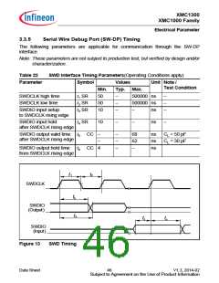
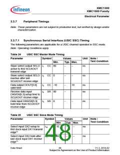
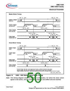
Master Mode Timing
t1
t2
Select Output
SELOx
Inactive
Inactive
Active
Clock Output
SCLKOUT
Receive
Edge
Last Receive
Edge
First Transmit
Edge
Transmit
Edge
t3
t3
Data Output
DOUT[3:0]
t4
t4
t5
t5
Data Input
DX0/DX[5:3]
Data
valid
Data
valid
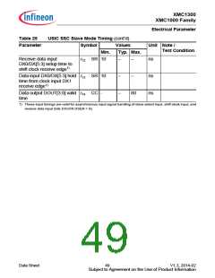
Slave Mode Timing
t10
t11
Select Input
DX2
Inactive
Active
Inactive
Clock Input
DX1
Receive
Edge
Last Receive
Edge
First Transmit
Edge
Transmit
Edge
t12
t12
t13
t13
Data Input
DX0/DX[5:3]
Data
valid
Data
valid
t14
t14
Data Output
DOUT[3:0]
Transmit Edge: with this clock edge, transmit data is shifted to transmit data output.
Receive Edge: with this clock edge, receive data at receive data input is latched.
Drawn for BRGH.SCLKCFG = 00B. Also valid for for SCLKCFG = 01B with inverted SCLKOUT signa.l
USIC_SSC_TMGX.VSD
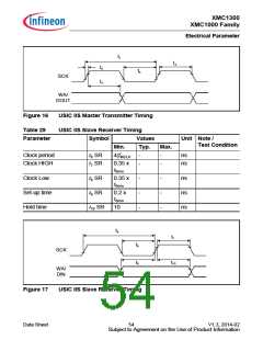
Figure 14
USIC - SSC Master/Slave Mode Timing
Note: This timing diagram shows a standard configuration, for which the slave select
signal is low-active, and the serial clock signal is not shifted and not inverted.
Data Sheet
50
V1.3, 2014-02
Subject to Agreement on the Use of Product Information

 INFINEON [ Infineon ]