TLE9879QXA40
Electrical Characteristics
29.2.4
VPRE Voltage Regulator (PMU Subblock) Parameters
The PMU VPRE Regulator acts as a supply of VDDP and VDDEXT voltage regulators.
Table 25
Functional Range
Parameter
Symbol
Values
Unit Note / Test Condition Number
Min.
Typ. Max.
1)
Specified output current
IVPRE
–
–
110
mA
P_2.4.1
1) Not subject to production test, specified by design.
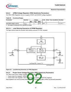
29.2.4.1 Load Sharing Scenarios of VPRE Regulator
The figure below shows the possible load sharing scenarios of VPRE regulator.
VS
VPRE
max. 110 mA
VDDEXT - 5V
1: max. 20 mA
2: max. 40 mA
VDDP - 5V
1: max. 90 mA
2: max. 70 mA
VDDEXT
VDDP
VDDC
CVDDEXT
CVDDP
GND (Pin 39)
GND (Pin 39)
VDDC - 1.5V
max. 40 mA
CVDDC
GND (Pin 39)
Load Sharing VPRE – Scenarios 1 & 2
Load_Sharing_VPRE.vsd
Figure 33 Load Sharing Scenarios of VPRE Regulator
29.2.5
Power Down Voltage Regulator (PMU Subblock) Parameters
The PMU Power Down voltage regulator consists of two subblocks:
•
•
Power Down Pre regulator: VDD5VPD
Power Down Core regulator: VDD1V5_PD (Supply used for GPUDATAxy registers)
Both regulators are used as purely internal supplies. The following table contains all relevant parameters:
Data Sheet
92
Rev. 1.0, 2015-04-30

 INFINEON [ Infineon ]