TLE9879QXA40
High-Speed Synchronous Serial Interface (SSC1/SSC2)
21.2
Introduction
The High-Speed Synchronous Serial Interface (SSC) supports both full-duplex and half-duplex serial synchronous
communication. The serial clock signal can be generated by the SSC internally (master mode), using its own 16-
bit baud rate generator, or can be received from an external master (slave mode). Data width, shift direction, clock
polarity, and phase are programmable. This allows communication with SPI-compatible devices or devices using
other synchronous serial interfaces.
Data is transmitted or received on TXD and RXD lines, which are normally connected to the MTSR
(MasterTransmit/Slave Receive) and MRST (Master Receive/Slave Transmit) pins. The clock signal is output via
line MS_CLK (Master Serial Shift Clock) or input via line SS_CLK (Slave Serial Shift Clock). Both lines are
normally connected to the pin SCLK. Transmission and reception of data are double-buffered.
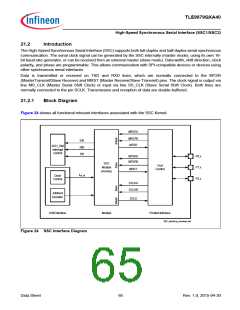
21.2.1
Block Diagram
Figure 24 shows all functional relevant interfaces associated with the SSC Kernel.
MRSTA
MRSTB
EIR
MTSR
SCU_DM
Interrupt
Control
RIR
TIR
MTSRA
MTSRB
P0.x
P1.x
P2.x
SSC
Port
Control
Module
(Kernel)
MRST
fhw_clk
Clock
Control
SCLKA
SCLKB
Address
Decoder
SCLK
AHB Interface
Module
ProductInterface
SSC_interface_overview.vsd
Figure 24 SSC Interface Diagram
Data Sheet
65
Rev. 1.0, 2015-04-30

 INFINEON [ Infineon ]