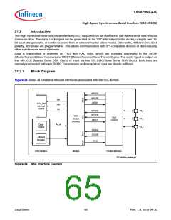
TLE9879QXA40
Measurement Core Module (incl. ADC2)
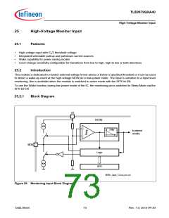
23
Measurement Core Module (incl. ADC2)
23.1
Features
•
•
•
•
8 individually programmable channels split into two groups of user configurable and non user configurable
Individually programmable channel prioritization scheme for measurement unit
Two independent filter stages with programmable low-pass and time filter characteristics for each channel
Two channel configurations:
– Programmable upper- and lower trigger thresholds comprising a fully programmable hysteresis
– Two individually programmable trigger thresholds with limit hysteresis settings
Individually programmable interrupts and statuses for all channel thresholds
•
23.2
Introduction
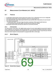
The basic function of this block is the digital postprocessing of several analog digitized measurement signals by
means of filtering, level comparison and interrupt generation. The measurement postprocessing block consists of
ten identical channel units attached to the outputs of the 10-channel 8-bit ADC (ADC2). It processes ten channels,
where the channel sequence and prioritization is programmable within a wide range.
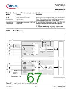
23.2.1
Block Diagram
4
/
Measurement Core Module
MUX_SEL<3:0>
Channel Controller
(Sequencer)
ADC2 - SFR
rfu
VS
CH0
CH1
CH2
CH3
CH4
CH5
CH6
CH7
CH8
CH9
VSD
VCP
1st Order IIR
1
/
+
-
8 Bit ADC
VREF
UP_X_STS
+ / -
+ / -
Calibration Unit:
y= a + (1+b)*x
THy_z_UPPER.
CHx
8
/
10
/
8
/
MON
MUX
A
D
VDDP
VAREF
PMU-VBG
VDDC
1
/
THy_z_LOWER.
CHx
-
LOW_X_STS
+
Digital Signal Processing
Temperature Sensor
TSENSE
Figure 27 Module Block Diagram
Data Sheet
69
Rev. 1.0, 2015-04-30

 INFINEON [ Infineon ]