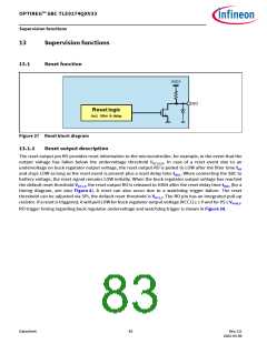
OPTIREG™ SBC TLE9274QXV33
Supervision functions
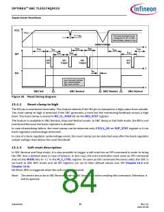
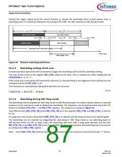
Should the trigger signal meet the closed window or should the watchdog timer period elapse, then a
watchdog reset is created by setting the reset output RO LOW. The SBC switches to SBC Restart mode.
tWD x 0.6
tWD x 0.9
Typ. closed window
Typ. open window
tWD x 0.48
tWD x 0.72
tWD x 1.0
tWD x 1.20
tWD x 1.80
closed window
uncertainty
open window
uncertainty
Watchdog Timer Period (WD_TIMER)
t / [tWD_TIMER
]
safe trigger area
Figure 40 Window watchdog definitions
13.2.3
Watchdog setting check sum
A check sum bit is part of the SPI command to trigger the watchdog and to set the watchdog setting.
The sum of the 8 bits in the register WD_CTRL needs to be even. This is realized by either setting the bit
CHECKSUM to “0” or “1”.
If the check sum is wrong the SPI command is ignored, i.e. the watchdog is not triggered or the settings are not
changed and the bit SPI_FAIL is set.
The checksum is calculated by taking all 8 data bits into account.
(13.1)
CHKSUM = Bit15
…
Bit8
13.2.4
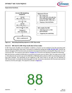
Watchdog during SBC Stop mode
The watchdog can be disabled for SBC Stop mode in SBC Normal mode. For safety reasons, there is a special
sequence to be ensured in order to disable the watchdog. The sequence can be implemented only if the FSI
feature is disabled (FSI_FO2 = 1 on HW_CTRL register). The sequence is shown in Figure 41.
Two different bits (WD_STM_ EN_0 and WD_STM_ EN_1) in the registers WD_CTRL and WK_CTRL_1 need to
be set.
If a sequence error occurs, then the bit WD_STM_ EN_1 is cleared and the sequence has to be started again.
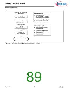
The watchdog can be enabled by triggering the watchdog in SBC Stop mode or by switching back to
SBC Normal mode via SPI. In both cases, the watchdog will start with a long open window and the bits
WD_STM_ EN_1 and WD_STM_ EN_0 are cleared. After the long open window, the watchdog has to be served
as configured in WD_CTRL register.
Note: The bit WD_STM_ EN_0 will be cleared automatically when the sequence is started and it was “1” before.
Datasheet
87
Rev.2.0
2022-05-06

 INFINEON [ Infineon ]