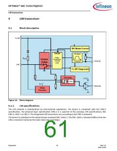
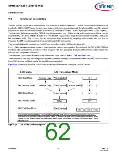
OPTIREG™ SBC TLE9274QXV33
LIN transceiver
register via SPI. No interrupt is generated when coming out of Sleep mode. The microcontroller can now
switch the LIN transceiver into LIN Normal mode via SPI to start communication.
9.2.5
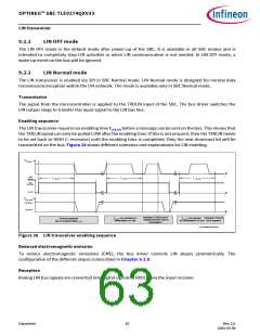
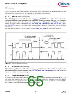
TXDLIN Time-out feature
If the TXDLIN signal is dominant for the time t > tBUS_LIN_TO, the TXDLIN time-out function deactivates the
LIN transmitter output stage temporarily. The transceiver remains in recessive state. The TXDLIN time-out
function prevents the LIN bus from being blocked by a permanent LOW signal on the TXDLIN pin caused by a
failure. The failure is stored in the SPI flag LIN1_FAIL, LIN2_FAIL, LIN3_FAIL and LIN4_FAIL on BUS_STAT_1
and BUS_STAT_2 registers. The LIN transmitter stage is activated again after the dominant time-out condition
is removed.
The TXDLIN time-out feature can be disabled with SPI bit LIN_TXD_ TO for all LINs at the same time.
Recovery of the
microcontroller error
TXDLIN Time-Out due to
microcontroller error
Release after TXDLIN
Time-out
Normal Communication
ttimeout
ttorec
Normal Communication
TXDLIN
t
LIN
t
Figure 27 TXDLIN time-out function
9.2.6
Bus dominant clamping
If the LIN bus signal is dominant for a time t > tBUS_LIN_TO in LIN Normal or Receive-Only mode, then a bus
dominant clamping is detected and the SPI bits LIN1_FAIL, LIN2_FAIL, LIN3_FAIL and LIN4_FAIL are set. The
transceiver configuration stays unchanged.
9.2.7
Undervoltage detection
In case the supply voltage VLIN is dropping below the VLIN undervoltage detection threshold (VLIN < VLIN,UVD),
the TLE9274QXV33 will set the LINx in Receive-Only mode (the transmitter is disabled). The receiver stage is
active. If the power supply VLIN reaches a higher level than the VLIN undervoltage detection threshold (VLIN >
V
LIN,UVD), the TLE9274QXV33 continues with normal operation.
Datasheet
65
Rev.2.0
2022-05-06

 INFINEON [ Infineon ]