OPTIREG™ SBC TLE9274QXV33
LIN transceiver
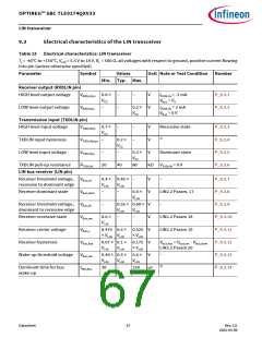
Table 15 Electrical characteristics: LIN transceiver (cont’d)
Tj = -40°C to +150°C, VLIN = 5.5 V to 18 V, RL = 500 Ω, all voltages with respect to ground, positive current flowing
into pin (unless otherwise specified)
Parameter
Symbol
Values
Unit Note or Test Condition Number
Min. Typ. Max.
LIN bus transmitter (LIN pin)
1)
Bus serial diode voltage drop Vserdiode 0.4
0.7
1.0
V
V
V
= VCC1
;
P_9.3.15
TXDLIN
LIN2.2 Param 21
Bus recessive output voltage VBUS,ro
0.8 ×
–
VLIN
VTXDLIN = high Level
P_9.3.16
P_9.3.20
P_9.3.21
VLIN
Bus short circuit current
IBUS,sc
40
100
150
mA VBUS = 18 V;
LIN2.2 Param 12
µA VLIN = 0 V;
-12 V ≤ VBUS ≤ 6 V;
LIN2.2 Param 15
µA VLIN = 0 V;
Leakage current
loss of ground
IBUS,lk1
-1000 -450 20
Leakage current
loss of battery
IBUS,lk2
IBUS,lk3
IBUS,lk4
–
–
20
–
P_9.3.22
P_9.3.23
P_9.3.24
P_9.3.25
0 V ≤ VBUS ≤ 18 V;
LIN2.2 Param 16
Leakage current
driver off
-1
–
–
mA VLIN = 18 V;
BUS = 0 V;
LIN2.2 Param 13
µA VLIN = 8 V;
BUS = 18 V;
V
Leakage current
driver off
–
20
47
V
LIN2.2 Param 14
Bus pull-up resistance
LIN input capacitance
RBUS
CBUS
20
30
kΩ Normal mode
LIN2.2 Param 26
1)
20
1
25
6
ρF
P_9.3.26
P_9.3.27
Receiver propagation delay td(L),R
bus dominant to RXDLIN
LOW
–
–
µs VCC = 5 V;
C
RXDLIN = 20 pF;
LIN2.2 Param 31
µs VCC = 5 V;
Receiver propagation delay td(H),R
1
6
P_9.3.28
bus recessive to RXDLIN HIGH
CRXDLIN = 20 pF;
LIN2.2 Param 31
Receiver delay symmetry
tsym,R
-2
8
–
2
µs tsym,R = td(L),R - td(H),R;
LIN2.2 Param 32
µs 2) time from enabling LIN P_9.3.39
P_9.3.29
LIN transceiver enabling time tLIN,EN
13
18
(CS HIGH) to first signal on
RXDLIN
1)2)
Bus dominant time out
tBUS_LIN
–
–
20
20
–
–
ms
ms
P_9.3.30
P_9.3.31
_TO
1)2)
TXDLIN dominant time out
tTXDLIN_LIN
V
= 0 V
TXDLIN
_TO
Datasheet
68
Rev.2.0
2022-05-06

 INFINEON [ Infineon ]