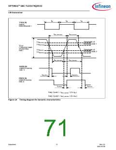
OPTIREG™ SBC TLE9274QXV33
LIN transceiver
9.3
Electrical characteristics of the LIN transceiver
Table 15 Electrical characteristics: LIN transceiver
Tj = -40°C to +150°C, VLIN = 5.5 V to 18 V, RL = 500 Ω, all voltages with respect to ground, positive current flowing
into pin (unless otherwise specified)
Parameter
Symbol
Values
Unit Note or Test Condition Number
Min. Typ. Max.
Receiver output (RXDLIN pin)
HIGH level output voltage
VRXDLIN,H 0.8 ×
–
–
–
V
V
IRXDLIN = -2 mA
bus = VS
IRXDLIN = 2 mA
bus = 0 V
P_9.3.1
P_9.3.2
VCC
V
LOW level output voltage
VRXDLIN,L
–
0.2 ×
VCC
V
Transmission input (TXDLIN pin)
HIGH level input voltage
TXDLIN input hysteresis
LOW level input voltage
VTXDLIN,H 0.7 ×
–
–
–
V
V
V
Recessive state
P_9.3.3
P_9.3.4
P_9.3.5
P_9.3.6
VCC
1)
VTXDLIN,hys
VTXDLIN,L
RTXDLIN
–
0.2 ×
VCC
–
–
0.3 ×
VCC
Dominant state
TXDLIN pull-up resistance
20
40
80
kΩ VTXDLIN = 0 V
LIN bus receiver (LIN pin)
Receiver threshold voltage, VBus,rd
recessive to dominant edge
0.4 × 0.45 × –
V
V
–
P_9.3.7
VLIN
VLIN
Receiver dominant state
VBus,dom
–
–
0.4 ×
LIN2.2 Param. 17
–
P_9.3.8
VLIN
Receiver threshold voltage, VBus,dr
–
0.55 × 0.60 × V
P_9.3.9
dominant to recessive edge
VLIN
VLIN
Receiver recessive state
Receiver center voltage
Receiver hysteresis
VBus,rec
VBus,c
0.6 ×
VLIN
–
–
V
LIN2.2 Param 18
LIN2.2 Param 19
P_9.3.10
P_9.3.11
P_9.3.12
P_9.3.13
P_9.3.14
0.475 0.5 × 0.525
× VLIN VLIN × VLIN
0.07 × 0.1 × 0.175
VLIN VLIN × VLIN
0.40 × 0.5 × 0.6 ×
V
VBus,hys
V
Vbus,hys = Vbus,rec - Vbus,dom
LIN2.2 Param 20
Wake-up threshold voltage VBus,wk
V
–
VLIN
VLIN
VLIN
2)
Dominant time for bus
wake-up
tWK,Bus
30
–
150
µs
Datasheet
67
Rev.2.0
2022-05-06

 INFINEON [ Infineon ]