OPTIREG™ SBC TLE9274QXV33
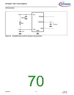
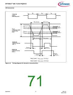
LIN transceiver
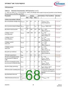
Table 15 Electrical characteristics: LIN transceiver (cont’d)
Tj = -40°C to +150°C, VLIN = 5.5 V to 18 V, RL = 500 Ω, all voltages with respect to ground, positive current flowing
into pin (unless otherwise specified)
Parameter
Symbol
Values
Unit Note or Test Condition Number
Min. Typ. Max.
1)2)
TXDLIN dominant time out
recovery time
ttorec
–
10
–
µs
P_9.3.32
Duty cycle D1
(For worst case at 20 kbit/s)
LIN2.2 normal slope
D1
0.396
–
–
3) THRec(max) = 0.744 × VS; P_9.3.33
THDom(max) = 0.581 × VS;
V
LIN = 7.0…18 V;
tbit = 50 µs;
D1 = tbus_rec(min)/2 tbit
LIN2.2 Param 27
;
Duty cycle D2
(for worst case at 20 kbit/s)
LIN2.2 normal slope
D2
D3
D4
–
–
–
–
0.581
3) THRec(min) = 0.422 × VS; P_9.3.34
THDom(min) = 0.284 × VS;
VLIN = 7.0…18 V;
tbit = 50 µs;
D2 = tbus_rec(max)/2 tbit
;
LIN2.2 Param 28
3) THRec(max) = 0.778 × VS; P_9.3.35
THDom(max) = 0.616 × VS;
Duty cycle D3
(for worst case at 10.4 kbit/s)
SAE J2602 low slope
0.417
–
V
LIN = 7.0…18 V;
tbit = 96 µs;
D3 = tbus_rec(min)/2 tbit
LIN2.2 Param 29
;
Duty cycle D4
(for worst case at 10.4 kbit/s)
SAE J2602 low slope
–
0.590
3) THRec(min) = 0.389 × VS; P_9.3.36
THDom(min) = 0.251 × VS;
VLIN = 7.0…18 V;
tbit =96 µs;
D4 = tbus_rec(max)/2 tbit
;
LIN2.2 Param 30
1) Not subject to production test, specified by design.
2) Not subject to production test, tolerance defined by internal oscillator tolerance.
3) Bus load conditions concerning LIN spec 2.2 CLIN, RLIN = 1 nF, 1 kΩ / 6.8 nF, 660 Ω / 10 nF, 500 Ω.
Datasheet
69
Rev.2.0
2022-05-06

 INFINEON [ Infineon ]