OPTIREG™ SBC TLE9274QXV33
High-speed CAN transceiver
Table 13 Electrical characteristics (cont’d)
Tj = -40°C to +150°C; VS = 5.5 V to 28 V; VCAN = 4.75 V to 5.25 V; RL = 60 Ω; CAN Normal mode; all voltages with
respect to ground, positive current flowing into pin (unless otherwise specified)
Parameter
Symbol
Values
Typ.
–
Unit Note or
Test Condition
Number
Min.
Max.
LOW level input voltage
threshold
VTXDCAN,L
0.3 ×
Vcc1
–
V
CAN Normal mode; P_8.3.22
dominant state
1)
TXDCAN input hysteresis
VTXDCAN,hys
–
0.12 ×
–
mV
P_8.3.23
Vcc1
TXDCAN pull-up resistance RTXDCAN
20
8
40
13
80
18
kΩ
-
P_8.3.24
CAN transceiver enabling
time
tCAN,EN
µs
7) CSN = HIGH to first P_8.3.25
valid transmitted
TXDCAN dominant
Dynamic CAN transceiver characteristics
Driver symmetry
VSYM
4.5
–
–
5.5
3.5
V
5) CAN Normal mode; P_8.3.45
VTXDCAN = 0 V / 5 V;
VSYM = VCANH + VCANL
V
CAN = 5 V;
CSPLIT = 4.7 nF;
50 Ω ≤ RL ≤ 60 Ω
Min. dominant time for bus tWake1
0.5
µs
-12 V ≤ VCM(CAN) ≤
P_8.3.26
wake-up
12 V;
V
diff ≤ 3 V
CAN Wake-capable
mode
Wake-up time-out, recessive tWake2
bus
0.5
–
–
–
10
ms
µs
7) CAN Wake-capable P_8.3.27
mode
7) CAN Wake-capable P_8.3.57
mode
BUS bias reaction time
tbias
250
V
CAN = 5 V;
CL = 100 pF;
GND = 100 pF;
C
RL = 60 Ω
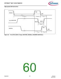
Loop delay
tLOOP,f
–
–
150
150
255
255
ns
ns
5) CAN Normal mode; P_8.3.28
CL = 100 pF;
RL = 60 Ω;
(recessive to dominant)
V
C
CAN = 5 V;
RXDCAN = 15 pF
Loop delay
tLOOP,r
5) CAN Normal mode; P_8.3.29
CL = 100 pF;
(dominant to recessive)
RL = 60 Ω;
V
C
CAN = 5 V;
RXDCAN = 15 pF
Datasheet
56
Rev.2.0
2022-05-06

 INFINEON [ Infineon ]