OPTIREG™ SBC TLE9274QXV33
DC/DC regulators
Table 10 Electrical characteristics (cont’d)
Tj = -40°C to +150°C; VS = 5.5 V to 28 V; all voltages with respect to ground, positive current flowing into pin
(unless otherwise specified)
Parameter
Symbol
Values
Unit Note or Test Condition
Number
Min. Typ. Max.
Boost voltage 2
VBST2_1
7.6
8
8.4
V
V
V
3) SBC Normal mode
SUP = 3 V
VS = 450 mA
Boost enabled
BOOST_V = 0
BOOST_VH = 0
P_6.5.6
V
I
Boost voltage 3
VBST3_1
9.5
10
7
10.5
7.5
3) SBC Normal mode
P_6.5.30
P_6.5.7
V
SUP = 3 V
IVS = 350 mA
Boost enabled
BOOST_V = 0
BOOST_VH = 1
Boost switch ON/OFF voltage 1 VBST,TH1
6.35
Boost enabled
VS falling
threshold
BOOST_V = 1
Boost switch ON/OFF
hysteresis 1
VBST,HYS1 300 500 600 mV
Boost enabled
BOOST_V = 1
P_6.5.8
Boost switch ON/OFF voltage 2 VBST,TH2
threshold
9.5
10
1
10.5
1.2
–
V
Boost enabled
VS falling; BOOST_V = 0
P_6.5.32
P_6.5.33
P_6.5.28
Boost switch ON/OFF
hysteresis 2
VBST,HYS2 0.9
V
Boost enabled;
BOOST_V = 0
2)
BSTG rise switching time
tBSTG,rise
–
–
30
ns
V
> 3 V
SUP
20% - 80%
C
BSTG = 470 pF
2)
BSTG fall switching time
tBSTG,fall
30
–
ns
V
> 3 V
P_6.5.29
SUP
20% - 80%
BSTG = 470 pF
Boost enable
SUP > 3 V
C
Overcurrent shunt voltage
threshold
VTH,SNS
fBST
199 210 221 mV
P_6.5.21
P_6.5.10
V
Boost switching frequency
Boost switch gate driver
Duration of PH1
405 450 495 kHz Normal mode (PWM)
2)
tPH1
tPH2
tPH3
tPH5
tPH6
tPH7
–
–
37.5
25
–
–
–
–
–
–
ns
ns
ns
ns
ns
ns
P_6.5.17
P_6.5.18
P_6.5.19
P_6.5.22
P_6.5.25
P_6.5.26
2)
2)
2)
2)
2)
Duration of PH2
Duration of PH3
124 131
Duration of PH5
–
62.5
25
Duration of PH6
–
Duration of PH7
29
31
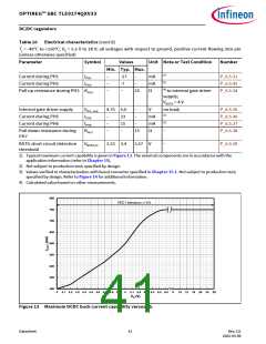
Datasheet
40
Rev.2.0
2022-05-06

 INFINEON [ Infineon ]