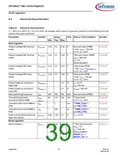
OPTIREG™ SBC TLE9274QXV33
DC/DC regulators
Table 10 Electrical characteristics (cont’d)
Tj = -40°C to +150°C; VS = 5.5 V to 28 V; all voltages with respect to ground, positive current flowing into pin
(unless otherwise specified)
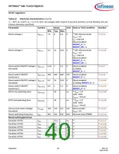
Parameter
Symbol
Values
Unit Note or Test Condition
Number
Min. Typ. Max.
2)
Current during PH1
Current during PH2
IPH1
IPH2
–
–
–
-27
-7
–
–
mA
P_6.5.31
P_6.5.42
P_6.5.34
2)
–
mA
Pull up resistance during PH3 RPH3
25
Ω
4) to internal gate driver
supply;
V
BSTG = 4 V
Internal gate driver supply
Current during PH5
Vdrv_sup
4.75 5.0
–
V
no load;
P_6.5.35
P_6.5.36
P_6.5.37
P_6.5.38
2)
IPH5
IPH6
RPH7
–
–
–
23
15
–
–
mA
mA
Ω
2)
Current during PH6
–
Pull down resistance during
PH7
15
–
BSTG short circuit detection
threshold
VBSTG,sc
3.23 3.4
3.57
V
–
P_6.5.39
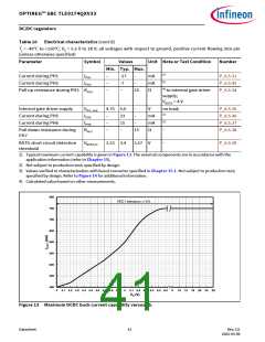
1) Typical maximum current capability is given in Figure 13. The external components are in accordance with the
application information (refer to Chapter 15).
2) Not subject to production test; specified by design.
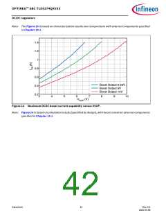
3) Values verified in characterization with boost converter specified in Chapter 15.1. Not subject to production test;
specified by design. Refer to Figure 14 for additional information.
4) Calculated value based on other measurements.
800
VCC1 tolerance +/-2%
750
700
650
600
550
500
450
400
4
4.1 4.2 4.3 4.4 4.5 4.6 4.7 4.8 4.9
5
5.1 5.2 5.3 5.4 5.5 6.5
VS (V)
8
10 12 18 20 24 28
Figure 13 Maximum DCDC buck current capability versus VS.
Datasheet
41
Rev.2.0
2022-05-06

 INFINEON [ Infineon ]