OPTIREG™ SBC TLE9274QXV33
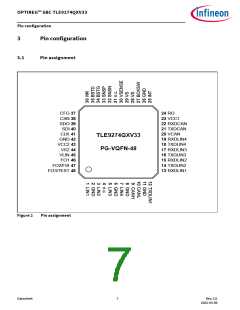
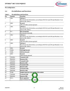
Pin configuration
3.2
Pin definitions and functions
Table 1
Pin definitions and functions
Pin
Symbol
Function
1
LIN1
LIN bus 1
Bus line for the LIN interface, according to ISO 9141 and LIN specification 2.1 as
well as SAE J2602-2
2
3
GND
LIN2
Ground
LIN1 and LIN2 common ground
LIN bus 2
Bus line for the LIN interface, according to ISO 9141 and LIN specification 2.1 as
well as SAE J2602-2
4
5
N.C.
Not connected
Not bonded internally
LIN3
LIN bus 3
Bus line for the LIN interface, according to ISO 9141 and LIN specification 2.1 as
well as SAE J2602-2
6
7
GND
LIN4
Ground
LIN3 and LIN4 common ground
LIN bus 4
Bus line for the LIN interface, according to ISO 9141 and LIN specification 2.1 as
well as SAE J2602-2
8
GND
Ground
9
CANH
CANL
GND
CAN high bus pin
CAN low bus pin
10
11
Ground
CAN common ground
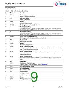
12
13
14
15
16
17
18
19
20
21
22
23
TXDLIN1
RXDLIN1
TXDLIN2
RXDLIN2
TXDLIN3
RXDLIN3
TXDLIN4
RXDLIN4
VCAN
Transmit LIN1
Receive LIN1
Transmit LIN2
Receive LIN2
Transmit LIN3
Receive LIN3
Transmit LIN4
Receive LIN4
Supply input for internal HS-CAN module
Transmit CAN
TXDCAN
RXDCAN
VCC1
Receive CAN
Buck regulator
Input feedback for buck regulator
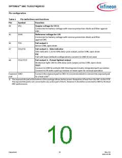
Datasheet
8
Rev.2.0
2022-05-06

 INFINEON [ Infineon ]